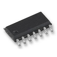
FM31274-G Ramtron, FM31274-G Datasheet - Page 8

FM31274-G
Manufacturer Part Number
FM31274-G
Description
FRAM, MPU SUPPORT, 16K, RTC, SOIC14
Manufacturer
Ramtron
Datasheet
1.FM31274-G.pdf
(26 pages)
Specifications of FM31274-G
Memory Size
16Kbit
Nvram Features
RTC
Supply Voltage Range
4V To 5.5V
Memory Case Style
SOIC
No. Of Pins
14
Operating Temperature Range
-40°C To +85°C
Interface
Serial
Package / Case
SOIC
Memory Configuration
2048 X 8
Interface Type
I2C, Serial, 2-Wire
Rohs Compliant
Yes
Lead Free Status / RoHS Status
Lead free / RoHS Compliant
Available stocks
Company
Part Number
Manufacturer
Quantity
Price
Company:
Part Number:
FM31274-GTR
Manufacturer:
CYPRESS
Quantity:
2 500
Part Number:
FM31274-GTR
Manufacturer:
RAMTRON
Quantity:
20 000
Calibration
When the CAL bit in a register 00h is set to 1, the
clock enters calibration mode. In calibration mode,
the CAL/PFO output pin is dedicated to the
calibration function and the power fail output is
temporarily unavailable. Calibration operates by
applying a digital correction to the counter based on
the frequency error. In this mode, the CAL/PFO pin
is driven with a 512 Hz (nominal) square wave. Any
measured deviation from 512 Hz translates into a
timekeeping error. The user converts the measured
error in ppm and writes the appropriate correction
value to the calibration register. The correction
factors are listed in the table below. Positive ppm
errors require a negative adjustment that removes
pulses. Negative ppm errors require a positive
correction that adds pulses. Positive ppm adjustments
have the CALS (sign) bit set to 1, where as negative
ppm adjustments have CALS = 0. After calibration,
the clock will have a maximum error of ± 2.17 ppm
or ± 0.09 minutes per month at the calibrated
temperature.
The calibration setting is stored in F-RAM so is not
lost should the backup source fail. It is accessed with
bits CAL.4-0 in register 01h. This value only can be
written when the CAL bit is set to a 1. To exit the
calibration mode, the user must clear the CAL bit to a
0. When the CAL bit is 0, the CAL/PFO pin will
revert to the power fail output function.
Crystal Oscillator
The crystal oscillator is designed to use a 12.5pF
crystal without the need for external components,
such as loading capacitors. The FM31L27x device
has built-in loading capacitors that match the crystal.
If a 32.768kHz crystal is not used, an external
oscillator may be connected to the FM31L27x.
Rev. 2.0
Jan. 2011
CF
Years
8 bits
32.768 kHz
Months
5 bits
Figure 9. Real-Time Clock Core Block Diagram
User Interface Registers
6 bits
Date
3 bits
Days
Oscillator
/OSCEN
Apply the oscillator to the X1 pin. Its high and low
voltage levels can be driven rail-to-rail or amplitudes
as low as approximately 500mV p-p.
proper operation, a DC bias must be applied to the
X2 pin. It should be centered between the high and
low levels on the X1 pin. This can be accomplished
with a voltage divider.
In the example, R1 and R2 are chosen such that the
X2 voltage is centered around the X1 oscillator drive
levels. If you wish to avoid the DC current, you may
choose to drive X1 with an external clock and X2
with an inverted clock using a CMOS inverter.
Layout Requirements
The X1 and X2 crystal pins employ very high
impedance circuits and the oscillator connected to
these pins can be upset by noise or extra loading. To
reduce RTC clock errors from signal switching noise,
a guard ring must be placed around these pads and
the guard ring grounded. SDA and SCL traces should
be routed away from the X1/X2 pads. The X1 and X2
trace lengths should be less than 5 mm. The use of a
ground plane on the backside or inner board layer is
preferred. See layout example. Red is the top layer,
green is the bottom layer.
FM31L278/L276/L274/L272 - 3V I2C Companion
Hours
6 bits
Figure 10. External Oscillator
Divider
Clock
Minutes
7 bits
FM31L27x
X1 X2
512 Hz
1 Hz
R2
R1
Seconds
Update
Logic
7 bits
W
Vdd
To ensure
Page 8 of 26
R


