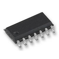
FM31274-G Ramtron, FM31274-G Datasheet - Page 18

FM31274-G
Manufacturer Part Number
FM31274-G
Description
FRAM, MPU SUPPORT, 16K, RTC, SOIC14
Manufacturer
Ramtron
Datasheet
1.FM31274-G.pdf
(26 pages)
Specifications of FM31274-G
Memory Size
16Kbit
Nvram Features
RTC
Supply Voltage Range
4V To 5.5V
Memory Case Style
SOIC
No. Of Pins
14
Operating Temperature Range
-40°C To +85°C
Interface
Serial
Package / Case
SOIC
Memory Configuration
2048 X 8
Interface Type
I2C, Serial, 2-Wire
Rohs Compliant
Yes
Lead Free Status / RoHS Status
Lead free / RoHS Compliant
Available stocks
Company
Part Number
Manufacturer
Quantity
Price
Company:
Part Number:
FM31274-GTR
Manufacturer:
CYPRESS
Quantity:
2 500
Part Number:
FM31274-GTR
Manufacturer:
RAMTRON
Quantity:
20 000
user desires to abort a write without altering the
memory contents, this should be done using a Start
or Stop condition prior to the 8
Memory Read Operation
There are two types of memory read operations. They
are current address read and selective address read. In
a current address read, the FM31L27x uses the
internal address latch to supply the address. In a
selective read, the user performs a procedure to first
set the address to a specific value.
Current Address & Sequential Read
As mentioned above the FM31L27x uses an internal
latch to supply the address for a read operation. A
current address read uses the existing value in the
address latch as a starting place for the read
operation. The system reads from the address
immediately following that of the last operation.
To perform a current address read, the bus master
supplies a slave address with the LSB set to 1. This
indicates that a read operation is requested. After
receiving
FM31L27x will begin shifting data out from the
current address on the next clock. The current address
is the value held in the internal address latch.
Beginning with the current address, the bus master
can read any number of bytes. Thus, a sequential read
is simply a current address read with multiple byte
transfers. After each byte the internal address counter
will be incremented.
Rev. 2.0
Jan. 2011
By FM31L27x
By Master
By FM31L27x
By Master
Start
the
S
Slave Address
complete
Start
S
Slave Address 0
0
device
th
A
data bit. The figures
Figure 15. Multiple Byte Memory Write
Address & Data
Address MSB
Figure 14. Single Byte Memory Write
address,
A
Address & Data
Acknowledge
Address MSB
the
A
Address LSB
Acknowledge
below illustrate a single- and multiple-writes to
memory.
There are four ways to terminate a read operation.
Failing to properly terminate the read will most likely
create a bus contention as the FM31L27x attempts to
read out additional data onto the bus. The four valid
methods follow.
1.
2.
3.
4.
If the internal address reaches the top of memory, it
will wrap around to 0000h on the next read cycle.
The figures below show the proper operation for
current address reads.
Selective (Random) Read
There is a simple technique that allows a user to
select a random address location as the starting point
for a read operation. This involves using the first
A
FM31L278/L276/L274/L272 - 3V I2C Companion
Each time the bus master acknowledges a byte,
this indicates that the FM31L27x should read
out the next sequential byte.
The bus master issues a NACK in the 9
cycle and a Stop in the 10
illustrated in the diagrams below and is
preferred.
The bus master issues a NACK in the 9
cycle and a Start in the 10
The bus master issues a Stop in the 9
cycle.
The bus master issues a Start in the 9
cycle.
Address LSB
A
Data Byte
A
A
Data Byte
th
.
th
clock cycle. This is
Data Byte
Page 18 of 26
A
Stop
th
th
P
th
th
clock
clock
clock
clock
A
Stop
P


