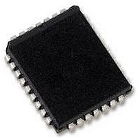
A29040BL-70F AMIC, A29040BL-70F Datasheet - Page 7

A29040BL-70F
Manufacturer Part Number
A29040BL-70F
Description
IC, SM, FLASH, 4MB, 5V
Manufacturer
AMIC
Datasheet
1.A29040BL-70F.pdf
(29 pages)
Specifications of A29040BL-70F
Memory Size
4Mbit
Supply Voltage Range
4.5V To 5.5V
Memory Case Style
PLCC
No. Of Pins
32
Access Time
70ns
Interface
Parallel
Logic Function Number
29040
Memory Configuration
512K X
Package / Case
PLCC
Memory Type
Uniform Sector Flash
Operating Temperature Range
0°C To +70°C
Rohs Compliant
Yes
Lead Free Status / RoHS Status
Lead free / RoHS Compliant
Available stocks
Company
Part Number
Manufacturer
Quantity
Price
Company:
Part Number:
A29040BL-70F
Manufacturer:
INTERSIL
Quantity:
140
Part Number:
A29040BL-70F
Manufacturer:
AMIC
Quantity:
20 000
Autoselect Mode
The autoselect mode provides manufacturer and device
identification, and sector protection verification, through
identifier codes output on I/O
intended for programming equipment to automatically match
a device to be programmed with its corresponding
programming algorithm. However, the autoselect codes can
also be accessed in-system through the command register.
When using programming equipment, the autoselect mode
requires V
pins A6, A1, and AO must be as shown in Autoselect Codes
(High Voltage Method) table. In addition, when verifying
sector protection, the sector address must appear on the
Sector Protection/Unprotection
The hardware sector protection feature disables both
program and erase operations in any sector. The hardware
sector unprotection feature re-enables both program and
erase operations in previously protected sectors.
Sector protection/unprotection must be implemented using
programming equipment. The procedure requires a high
voltage (V
The device is shipped with all sectors unprotected.
It is possible to determine whether a sector is protected or
unprotected. See "Autoselect Mode" for details.
Hardware Data Protection
The requirement of command unlocking sequence for
programming or erasing provides data protection against
inadvertent writes (refer to the Command Definitions table).
In addition, the following hardware data protection measures
prevent accidental erasure or programming, which might
otherwise be caused by spurious system level signals during
V
is powered up to read array data to avoid accidentally writing
data to the array.
Write Pulse "Glitch" Protection
Noise pulses of less than 5ns (typical) on
do not initiate a write cycle.
Logical Inhibit
Write cycles are inhibited by holding any one of
(January, 2007, Version 1.0)
CE
WE
Manufacturer ID: AMIC
Device ID: A29040B
Sector Protection
Verification
Continuation ID
CC
power-up transitions, or from system noise. The device
= V
must be a logical zero while
Description
IH
ID
ID
or
) on address pin A9 and the control pins.
(11.5V to 12.5 V) on address pinA9. Address
WE
= V
IH
. To initiate a write cycle,
Table 3. A29040B Autoselect Codes (High Voltage Method)
A18 - A16 A15 - A10
Address
7
Sector
- I/O
X
X
X
OE
0
. This mode is primarily
is a logical one.
OE
X
X
X
X
,
CE
OE
CE
or
V
V
V
V
A9 A8 - A7
ID
ID
ID
ID
=V
WE
and
IL
,
X
X
X
X
6
appropriate highest order address bits. Refer to the
corresponding Sector Address Tables. The Command
Definitions table shows the remaining address bits that are
don't care. When all necessary bits have been set as
required, the programming equipment may then read the
corresponding identifier code on I/O
autoselect codes in-system, the host system can issue the
autoselect command via the command register, as shown in
the Command Definitions table. This method does not
require V
the autoselect mode.
Power-Up Write Inhibit
If
device does not accept commands on the rising edge of
reading array data on the initial power-up.
Command Definitions
Writing specific address and data commands or sequences
into the command register initiates device operations. The
Command Definitions table defines the valid register
command sequences. Writing incorrect address and data
values or writing them in the improper sequence resets the
device to reading array data.
All addresses are latched on the falling edge of
whichever happens later. All data is latched on the rising
edge of
appropriate timing diagrams in the "AC Characteristics"
section.
Reading Array Data
The device is automatically set to reading array data
after device power-up. No commands are required to
retrieve data. The device is also ready to read array
data after completing an Embedded Program or
Embedded Erase algorithm. After the device accepts
an Erase Suspend command, the device enters the
Erase Suspend mode. The system can read array
data using the standard read timings, except that if it
reads at an address within erase-suspended sectors,
the device outputs status data. After completing a
programming operation in the Erase Suspend mode, the
WE
V
V
V
A6
V
WE
IL
IL
IL
IL
. The internal state machine is automatically reset to
A5 - A2
=
WE
ID
. See "Command Definitions" for details on using
CE
X
X
X
X
or
= V
CE
V
V
A1
V
V
IL
IH
IL
IL
IH
, whichever happens first. Refer to the
and
V
V
AO
V
V
IL
IH
IL
AMIC Technology, Corp.
IH
OE
= V
A29040B Series
Identifier Code on
00h (unprotected)
IH
01h (protected)
7
during power up, the
- I/O
I/O
86h
37h
7
- I/O
7Fh
0
.To access the
0
WE
or
CE
,


