A29040BL-70F AMIC, A29040BL-70F Datasheet - Page 22
A29040BL-70F
Manufacturer Part Number
A29040BL-70F
Description
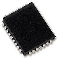
IC, SM, FLASH, 4MB, 5V
Manufacturer
AMIC
Datasheet
1.A29040BL-70F.pdf
(29 pages)
Specifications of A29040BL-70F
Memory Size
4Mbit
Supply Voltage Range
4.5V To 5.5V
Memory Case Style
PLCC
No. Of Pins
32
Access Time
70ns
Interface
Parallel
Logic Function Number
29040
Memory Configuration
512K X
Package / Case
PLCC
Memory Type
Uniform Sector Flash
Operating Temperature Range
0°C To +70°C
Rohs Compliant
Yes
Lead Free Status / RoHS Status
Lead free / RoHS Compliant
Available stocks
Company
Part Number
Manufacturer
Quantity
Price
Company:

Part Number:
A29040BL-70F
Manufacturer:
INTERSIL
Quantity:
140
Part Number:
A29040BL-70F
Manufacturer:
AMIC
Quantity:
20 000


Notes:
1. Typical program and erase times assume the following conditions: 25°C, 5.0V VCC, 100,000 cycles. Additionally,
2. Under worst case conditions of 90°C, VCC = 4.5V (4.75V for -55), 100,000 cycles.
3. The typical chip programming time is considerably less than the maximum chip programming time listed, since most bytes
4. In the pre-programming step of the Embedded Erase algorithm, all bytes are programmed to 00h before erasure.
5. System-level overhead is the time required to execute the four-bus-cycle command sequence for programming. See Table 4
6. The device has a guaranteed minimum erase and program cycle endurance of 100,000 cycles.
Timing Waveforms for Alternate CE Controlled Write Operation
Erase and Programming Performance
(January, 2007, Version 1.0)
Sector Erase Time
Chip Erase Time
Byte Programming Time
Chip Programming Time (Note 3)
programming typically assumes checkerboard pattern.
program faster than the maximum byte program time listed. If the maximum byte program time given is exceeded, only then
does the device set I/O
for further information on command definitions.
Addresses
Data
Note :
1. PA = Program Address, PD = Program Data, SA = Sector Address, I/O
2. Figure indicates the last two bus cycles of the command sequence.
WE
OE
CE
Parameter
t
RH
t
t
WS
GHEL
555 for program
2AA for erase
5
= 1. See the section on I/O
A0 for program
55 for erase
t
WC
t
t
CP
DS
PA for program
SA for sector erase
555 for chip erase
Typ. (Note 1)
t
t
t
DH
WH
CPH
t
AS
3.6
35
1
8
PD for program
30 for sector erase
10 for chip erase
5
for further information.
Max. (Note 2)
t
AH
t
21
BUSY
10.8
300
64
8
Data Polling
t
WHWH1 or 2
7
= Complement of Data Input, D
Unit
sec
sec
sec
µs
PA
AMIC Technology, Corp.
I/O
Excludes 00h programming
prior to erasure (Note 4)
Excludes system-level
overhead (Note 5)
7
A29040B Series
Comments
OUT
D
OUT
= Array Data.
Related parts for A29040BL-70F
Image
Part Number
Description
Manufacturer
Datasheet
Request
R


Part Number:
Description:
512K X 8 Bit CMOS 5.0 Volt-only, Uniform Sector Flash Memory
Manufacturer:
AMICC [AMIC Technology]
Datasheet:
Part Number:
Description:
2m X 16 Bit X 4 Banks Synchronous Dram - Amic Technology
Manufacturer:
AMIC Technology Corporation
Datasheet:

Part Number:
Description:
58T1324
Manufacturer:
AMIC
Datasheet:
Part Number:
Description:
Manufacturer:
AMIC Technology Corporation
Datasheet:
Part Number:
Description:
Manufacturer:
AMIC Technology Corporation
Datasheet:
Part Number:
Description:
Manufacturer:
AMIC Technology Corporation
Datasheet:
Part Number:
Description:
Manufacturer:
AMIC Technology Corporation
Datasheet:
Part Number:
Description:
Manufacturer:
AMIC Technology Corporation
Datasheet:
Part Number:
Description:
Manufacturer:
AMIC Technology Corporation
Datasheet:
Part Number:
Description:
Manufacturer:
AMIC Technology Corporation
Datasheet:
Part Number:
Description:
Manufacturer:
AMIC Technology Corporation
Datasheet:
Part Number:
Description:
Manufacturer:
AMIC Technology Corporation
Datasheet:
Part Number:
Description:
Manufacturer:
AMIC Technology Corporation
Datasheet:
Part Number:
Description:
Manufacturer:
AMIC Technology Corporation
Datasheet: