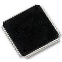
LFXP6C-5TN144C LATTICE SEMICONDUCTOR, LFXP6C-5TN144C Datasheet - Page 61

LFXP6C-5TN144C
Manufacturer Part Number
LFXP6C-5TN144C
Description
FPGA, 1.8V FLASH, INSTANT ON, SMD
Manufacturer
LATTICE SEMICONDUCTOR
Series
LatticeXPr
Datasheet
1.LFXP3C-3QN208C.pdf
(130 pages)
Specifications of LFXP6C-5TN144C
No. Of Logic Blocks
720
No. Of Macrocells
3000
Family Type
LatticeXP
No. Of Speed Grades
5
No. Of I/o's
100
Clock Management
PLL
Core Supply Voltage Range
1.71V To 3.465V
Lead Free Status / RoHS Status
Lead free / RoHS Compliant
Available stocks
Company
Part Number
Manufacturer
Quantity
Price
Company:
Part Number:
LFXP6C-5TN144C
Manufacturer:
LATTICE
Quantity:
2 291
Company:
Part Number:
LFXP6C-5TN144C
Manufacturer:
Lattice
Quantity:
60
Company:
Part Number:
LFXP6C-5TN144C
Manufacturer:
Lattice Semiconductor Corporation
Quantity:
10 000
Company:
Part Number:
LFXP6C-5TN144C-4I
Manufacturer:
LATTICE
Quantity:
2 291
Lattice Semiconductor
Signal Descriptions (Cont.)
Test and Programming (Dedicated pins. Pull-up is enabled on input pins during configuration.)
TMS
TCK
TDI
TDO
V
Configuration Pads (used during sysCONFIG)
CFG[1:0]
INITN
PROGRAMN
DONE
CCLK
BUSY
CSN
CS1N
WRITEN
D[7:0]
DOUT, CSON
DI
SLEEPN
TOE
1. Applies toþ LFXP10, LFXP15 and LFXP20 only.
2. Applies to LFXP “C” devices only.
3. Applies to LFXP “E” devices only.
CCJ
3
2
Signal Name
I/O
I/O
I/O
I/O Configuration Clock for configuring an FPGA in sysCONFIG mode.
I/O Generally not used. After configuration it is a user-programmable I/O pin.
I/O
—
O
O
I
I
I
I
I
I
I
I
I
I
I
Test Mode Select input, used to control the 1149.1 state machine.
Test Clock input pin, used to clock the 1149.1 state machine.
Test Data in pin, used to load data into device using 1149.1 state machine.
After power-up, this TAP port can be activated for configuration by sending
appropriate command. (Note: once a configuration port is selected it is
locked. Another configuration port cannot be selected until the power-up
sequence).
Output pin -Test Data out pin used to shift data out of device using 1149.1.
V
Mode pins used to specify configuration modes values latched on rising edge
of INITN. During configuration, a pull-up is enabled.
Open Drain pin - Indicates the FPGA is ready to be configured. During con-
figuration, a pull-up is enabled. If CFG1 and CFG0 are high (SDM) then this
pin is pulled low.
Initiates configuration sequence when asserted low. This pin always has an
active pull-up.
Open Drain pin - Indicates that the configuration sequence is complete, and
the startup sequence is in progress.
sysCONFIG chip select (Active low). During configuration, a pull-up is
enabled. After configuration it is user a programmable I/O pin.
sysCONFIG chip select (Active Low). During configuration, a pull-up is
enabled. After configuration it is user programmable I/O pin
Write Data on Parallel port (Active low). After configuration it is a user pro-
grammable I/O pin
sysCONFIG Port Data I/O. After configuration these are user programmable
I/O pins.
Output for serial configuration data (rising edge of CCLK) when using sys-
CONFIG port. After configuration, it is a user-programmable I/O pin.
Input for serial configuration data (clocked with CCLK) when using sysCON-
FIG port. During configuration, a pull-up is enabled. After configuration it is a
user-programmable I/O pin.
Sleep Mode pin - Active low sleep pin.þ When this pin is held high, the device
operates normally.þ When driven low, the device moves into Sleep Mode
after a specified time.This pin has a weak internal pull-up, but when not used
an external pull-up to V
Test Output Enable tri-states all I/O pins when driven low. This pin has a
weak internal pull-up, but when not used an external pull-up to V
mended.
CCJ
- The power supply pin for JTAG Test Access Port.
4-2
CC
is recommended.
Descriptions
LatticeXP Family Data Sheet
Pinout Information
CC
is recom-


