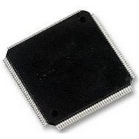
LFXP6C-5TN144C LATTICE SEMICONDUCTOR, LFXP6C-5TN144C Datasheet - Page 13

LFXP6C-5TN144C
Manufacturer Part Number
LFXP6C-5TN144C
Description
FPGA, 1.8V FLASH, INSTANT ON, SMD
Manufacturer
LATTICE SEMICONDUCTOR
Series
LatticeXPr
Datasheet
1.LFXP3C-3QN208C.pdf
(130 pages)
Specifications of LFXP6C-5TN144C
No. Of Logic Blocks
720
No. Of Macrocells
3000
Family Type
LatticeXP
No. Of Speed Grades
5
No. Of I/o's
100
Clock Management
PLL
Core Supply Voltage Range
1.71V To 3.465V
Lead Free Status / RoHS Status
Lead free / RoHS Compliant
Available stocks
Company
Part Number
Manufacturer
Quantity
Price
Company:
Part Number:
LFXP6C-5TN144C
Manufacturer:
LATTICE
Quantity:
2 291
Company:
Part Number:
LFXP6C-5TN144C
Manufacturer:
Lattice
Quantity:
60
Company:
Part Number:
LFXP6C-5TN144C
Manufacturer:
Lattice Semiconductor Corporation
Quantity:
10 000
Company:
Part Number:
LFXP6C-5TN144C-4I
Manufacturer:
LATTICE
Quantity:
2 291
Lattice Semiconductor
Figure 2-10. PLL Diagram
Figure 2-11 shows the available macros for the PLL. Table 2-11 provides signal description of the PLL Block.
Figure 2-11. PLL Primitive
Table 2-5. PLL Signal Descriptions
CLKI
CLKFB
RST
CLKOS
CLKOP
CLKOK
LOCK
DDAMODE
DDAIZR
DDAILAG
DDAIDEL[2:0]
DDAOZR
DDAOLAG
DDAODEL[2:0]
Signal
CLKFB
from CLKOP
(PLL internal),
from clock net
(CLKOP) or
from a user
clock (PIN or logic)
(from routing or
external pin)
CLKI
RST
CLKFB
CLKI
I/O
O
O
O
O
O
O
O
I
I
I
I
I
I
I
Input Clock
Divider
(CLKI)
EPLLB
Clock input from external pin or routing
PLL feedback input from CLKOP (PLL internal), from clock net (CLKOP) or from a user clock
(PIN or logic)
“1” to reset input clock divider
PLL output clock to clock tree (phase shifted/duty cycle changed)
PLL output clock to clock tree (No phase shift)
PLL output to clock tree through secondary clock divider
“1” indicates PLL LOCK to CLKI
Dynamic Delay Enable. “1” Pin control (dynamic), “0”: Fuse Control (static)
Dynamic Delay Zero. “1”: delay = 0, “0”: delay = on
Dynamic Delay Lag/Lead. “1”: Lag, “0”: Lead
Dynamic Delay Input
Dynamic Delay Zero Output
Dynamic Delay Lag/Lead Output
Dynamic Delay Output
Feedback
(CLKFB)
Divider
Dynamic Delay Adjustment
CLKOP
LOCK
Adjust
Delay
DDAIDEL[2:0]
DDA MODE
Controlled
Oscillator
DDAILAG
2-10
Voltage
DDAIZR
VCO
CLKFB
CLKI
RST
Description
Post Scalar
(CLKOP)
Divider
EHXPLLB
LatticeXP Family Data Sheet
Phase/Duty
Secondary
(CLKOK)
Divider
CLKOP
CLKOS
CLKOK
LOCK
DDAOZR
DDAOLAG
DDAODEL[2:0]
Select
Clock
Architecture
LOCK
CLKOS
CLKOP
CLKOK


