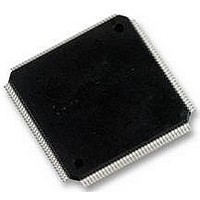
LFXP6C-5TN144C LATTICE SEMICONDUCTOR, LFXP6C-5TN144C Datasheet - Page 22

LFXP6C-5TN144C
Manufacturer Part Number
LFXP6C-5TN144C
Description
FPGA, 1.8V FLASH, INSTANT ON, SMD
Manufacturer
LATTICE SEMICONDUCTOR
Series
LatticeXPr
Datasheet
1.LFXP3C-3QN208C.pdf
(130 pages)
Specifications of LFXP6C-5TN144C
No. Of Logic Blocks
720
No. Of Macrocells
3000
Family Type
LatticeXP
No. Of Speed Grades
5
No. Of I/o's
100
Clock Management
PLL
Core Supply Voltage Range
1.71V To 3.465V
Lead Free Status / RoHS Status
Lead free / RoHS Compliant
Available stocks
Company
Part Number
Manufacturer
Quantity
Price
Company:
Part Number:
LFXP6C-5TN144C
Manufacturer:
LATTICE
Quantity:
2 291
Company:
Part Number:
LFXP6C-5TN144C
Manufacturer:
Lattice
Quantity:
60
Company:
Part Number:
LFXP6C-5TN144C
Manufacturer:
Lattice Semiconductor Corporation
Quantity:
10 000
Company:
Part Number:
LFXP6C-5TN144C-4I
Manufacturer:
LATTICE
Quantity:
2 291
Lattice Semiconductor
Figure 2-23. Output Register Block
Figure 2-24. ODDRXB Primitive
Tristate Register Block
The tristate register block provides the ability to register tri-state control signals from the core of the device before
they are passed to the sysIO buffers. The block contains a register for SDR operation and an additional latch for
DDR operation. Figure 2-25 shows the diagram of the Tristate Register Block.
In SDR mode, ONEG1 feeds one of the flip-flops that then feeds the output. The flip-flop can be configured a D-
type or latch. In DDR mode, ONEG1 is fed into one register on the positive edge of the clock and OPOS1 is
latched. A multiplexer running off the same clock selects the correct register for feeding to the output (D0).
Routing
From
ONEG0
OPOS0
CLK1
*Latch is transparent when input is low.
CLK
LSR
DA
DB
/LATCH
D
D
D-Type
LATCH
LE*
ODDRXB
2-19
Q
Q
Q
0
1
Programmed
Control
LatticeXP Family Data Sheet
OUTDDN
0
1
To sysIO
Buffer
DO
Architecture


