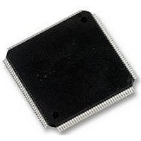
LFXP6C-5TN144C LATTICE SEMICONDUCTOR, LFXP6C-5TN144C Datasheet - Page 2

LFXP6C-5TN144C
Manufacturer Part Number
LFXP6C-5TN144C
Description
FPGA, 1.8V FLASH, INSTANT ON, SMD
Manufacturer
LATTICE SEMICONDUCTOR
Series
LatticeXPr
Datasheet
1.LFXP3C-3QN208C.pdf
(130 pages)
Specifications of LFXP6C-5TN144C
No. Of Logic Blocks
720
No. Of Macrocells
3000
Family Type
LatticeXP
No. Of Speed Grades
5
No. Of I/o's
100
Clock Management
PLL
Core Supply Voltage Range
1.71V To 3.465V
Lead Free Status / RoHS Status
Lead free / RoHS Compliant
Available stocks
Company
Part Number
Manufacturer
Quantity
Price
Company:
Part Number:
LFXP6C-5TN144C
Manufacturer:
LATTICE
Quantity:
2 291
Company:
Part Number:
LFXP6C-5TN144C
Manufacturer:
Lattice
Quantity:
60
Company:
Part Number:
LFXP6C-5TN144C
Manufacturer:
Lattice Semiconductor Corporation
Quantity:
10 000
Company:
Part Number:
LFXP6C-5TN144C-4I
Manufacturer:
LATTICE
Quantity:
2 291
www.latticesemi.com
© 2007 Lattice Semiconductor Corp. All Lattice trademarks, registered trademarks, patents, and disclaimers are as listed at www.latticesemi.com/legal. All other brand
or product names are trademarks or registered trademarks of their respective holders. The specifications and information herein are subject to change without notice.
July 2007
Features
Non-volatile, Infinitely Reconfigurable
Sleep Mode
TransFR™ Reconfiguration (TFR)
Extensive Density and Package Options
Embedded and Distributed Memory
Table 1-1. LatticeXP Family Selection Guide
PFU/PFF Rows
PFU/PFF Columns
PFU/PFF (Total)
LUTs (K)
Distributed RAM (KBits)
EBR SRAM (KBits)
EBR SRAM Blocks
V
PLLs
Max. I/O
Packages and I/O Combinations:
100-pin TQFP (14 x 14 mm)
144-pin TQFP (20 x 20 mm)
208-pin PQFP (28 x 28 mm)
256-ball fpBGA (17 x 17 mm)
388-ball fpBGA (23 x 23 mm)
484-ball fpBGA (23 x 23 mm)
CC
Voltage
• Instant-on – powers up in microseconds
• No external configuration memory
• Excellent design security, no bit stream to
• Reconfigure SRAM based logic in milliseconds
• SRAM and non-volatile memory programmable
• Allows up to 1000x static current reduction
• In-field logic update while system operates
• 3.1K to 19.7K LUT4s
• 62 to 340 I/Os
• Density migration supported
• 54 Kbits to 396 Kbits sysMEM™ Embedded
• Up to 79 Kbits distributed RAM
• Flexible memory resources:
intercept
through system configuration and JTAG ports
Block RAM
Distributed and block memory
Device
1.2/1.8/2.5/3.3V
LFXP3
384
136
136
100
16
24
12
54
62
3
6
2
1.2/1.8/2.5/3.3V
LFXP6
720
188
100
142
188
24
30
23
72
LatticeXP Family Data Sheet
6
8
2
1-1
Flexible I/O Buffer
Dedicated DDR Memory Support
sysCLOCK™ PLLs
System Level Support
• Programmable sysIO™ buffer supports wide
• Implements interface up to DDR333 (166MHz)
• Up to 4 analog PLLs per device
• Clock multiply, divide and phase shifting
• IEEE Standard 1149.1 Boundary Scan, plus
• Onboard oscillator for configuration
• Devices operate with 3.3V, 2.5V, 1.8V or 1.2V
1.2/1.8/2.5/3.3V
range of interfaces:
ispTRACY™ internal logic analyzer capability
power supply
LVCMOS 3.3/2.5/1.8/1.5/1.2
LVTTL
– SSTL 18 Class I
SSTL 3/2 Class I, II
– HSTL15 Class I, III
HSTL 18 Class I, II, III
PCI
LVDS, Bus-LVDS, LVPECL, RSDS
LFXP10
1216
216
244
188
244
32
38
10
39
24
4
1.2/1.8/2.5/3.3V
LFXP15
1932
324
300
188
268
300
40
48
15
61
36
Introduction
4
DS1001 Introduction_01.5
Data Sheet DS1001
1.2/1.8/2.5/3.3V
LFXP20
2464
396
340
188
268
340
44
56
20
79
44
4


