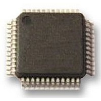
SC16C752BIB48 NXP Semiconductors, SC16C752BIB48 Datasheet - Page 29

SC16C752BIB48
Manufacturer Part Number
SC16C752BIB48
Description
IC, UART, DUAL, 64BYTE FIFO, 16C752
Manufacturer
NXP Semiconductors
Datasheet
1.SC16C752BIBS128.pdf
(47 pages)
Specifications of SC16C752BIB48
No. Of Channels
2
Data Rate
5Mbps
Supply Voltage Range
2.25V To 5.5V
Operating Temperature Range
-40°C To +85°C
Digital Ic Case Style
LQFP
No. Of Pins
48
Svhc
No SVHC (18-Jun-2010)
Uart Features
DMA Signalling Capability, Software Selectable Baud Rate Generator
Rohs Compliant
Yes
Lead Free Status / RoHS Status
Lead free / RoHS Compliant
Available stocks
Company
Part Number
Manufacturer
Quantity
Price
Company:
Part Number:
SC16C752BIB48
Manufacturer:
NXP Semiconductors
Quantity:
1 940
Company:
Part Number:
SC16C752BIB48
Manufacturer:
TI
Quantity:
430
Part Number:
SC16C752BIB48
Manufacturer:
NXP/恩智浦
Quantity:
20 000
Company:
Part Number:
SC16C752BIB48,128
Manufacturer:
NXP Semiconductors
Quantity:
10 000
Company:
Part Number:
SC16C752BIB48,151
Manufacturer:
NXP Semiconductors
Quantity:
10 000
Company:
Part Number:
SC16C752BIB48,157
Manufacturer:
NXP Semiconductors
Quantity:
10 000
NXP Semiconductors
SC16C752B
Product data sheet
7.12 Transmission Control Register (TCR)
7.11 Divisor latches (DLL, DLM)
Table 19.
These are two 8-bit registers which store the 16-bit divisor for generation of the baud clock
in the baud rate generator. DLM stores the most significant part of the divisor. DLL stores
the least significant part of the divisor.
Note that DLL and DLM can only be written to before Sleep mode is enabled, i.e., before
IER[4] is set.
This 8-bit register is used to store the receive FIFO threshold levels to stop/start
transmission during hardware/software flow control.
Register bit settings.
Table 20.
TCR trigger levels are available from 0 bytes to 60 bytes with a granularity of four.
Remark: TCR can only be written to when EFR[4] = logic 1 and MCR[6] = logic 1. The
programmer must program the TCR such that TCR[3:0] > TCR[7:4]. There is no built-in
hardware check to make sure this condition is met. Also, the TCR must be programmed
with this condition before auto-RTS or software flow control is enabled to avoid spurious
operation of the device.
Bit
5
4
3:0
Bit
7:4
3:0
Symbol
EFR[5]
EFR[4]
EFR[3:0] Combinations of software flow control can be selected by programming these bits.
Symbol
TCR[7:4]
TCR[3:0]
Enhanced Feature Register bits description
Transmission Control Register bits description
Description
Special character detect.
Enhanced functions enable bit.
See
All information provided in this document is subject to legal disclaimers.
logic 0 = special character detect disabled (normal default condition)
logic 1 = special character detect enabled. Received data is compared with
Xoff2 data. If a match occurs, the received data is transferred to FIFO and IIR[4]
is set to a logic 1 to indicate a special character has been detected.
logic 0 = disables enhanced functions and writing to IER[7:4], FCR[5:4],
MCR[7:5]
logic 1 = enables the enhanced function IER[7:4], FCR[5:4], and MCR[7:5] can
be modified, i.e., this bit is therefore a write enable.
5 V, 2.2 V and 2.5 V dual UART, 5 Mbit/s (max.), with 64-byte FIFOs
Table 3 “Software flow control options
Description
receive FIFO trigger level to resume transmission (0 to 60).
receive FIFO trigger level to halt transmission (0 to 60).
Rev. 6 — 30 November 2010
Table 20
…continued
(EFR[0:3])”.
shows Transmission Control
SC16C752B
© NXP B.V. 2010. All rights reserved.
29 of 47


