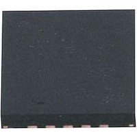
LTC4160EUDC-1#PBF Linear Technology, LTC4160EUDC-1#PBF Datasheet - Page 26

LTC4160EUDC-1#PBF
Manufacturer Part Number
LTC4160EUDC-1#PBF
Description
IC, BATT CHRG, Li-Ion, Li-Polymer, 1.2A, QFN20
Manufacturer
Linear Technology
Datasheet
1.LTC4160EUDC-1PBF.pdf
(32 pages)
Specifications of LTC4160EUDC-1#PBF
Battery Type
Li-Ion, Li-Polymer
Input Voltage
5.5V
Battery Charge Voltage
4.1V
Charge Current Max
1.2A
Battery Ic Case Style
QFN
No. Of Pins
20
No. Of Series Cells
1
Rohs Compliant
Yes
Lead Free Status / RoHS Status
Lead free / RoHS Compliant
Lead Free Status / RoHS Status
Lead free / RoHS Compliant
Available stocks
Company
Part Number
Manufacturer
Quantity
Price
LTC4160/LTC4160-1
APPLICATIONS INFORMATION
This same current pulse must not raise V
than 2V when connected to a standard host which must
have at least 96μF . The 96μF for a standard host represents
the minimum capacitance with V
5.25V. Since the SRP pulse must not drive V
than 2V, the capacitance seen at these voltage levels can be
greater than 96μF , especially if MLCCs are used. Therefore,
the 96μF represents a lower bound on the standard host
bypass capacitance for determining the amplitude and
duration of the current pulse. More capacitance will only
decrease the maximum level that V
given current pulse.
Figure 9 shows an On-The-Go device using the LTC4160/
LTC4160-1 acting as the A device. Additional capacitance
can be placed on the V
1 when using the overvoltage protection circuit. The B
device may not be able to distinguish between a powered
down LTC4160/LTC4160-1 with overvoltage protection
and a powered down standard host because of this extra
capacitance. In addition, if the SRP pulse raises V
above its UVLO threshold of 4.3V the LTC4160/LTC4160-1
will assume input power is available and will not attempt
to drive V
The-Go device using the LTC4160/LTC4160-1 respond to
data-line pulsing.
When an On-The-Go device using the LTC4160/LTC4160-1
becomes the B device, as in Figure 10, it must send out
a data line pulse followed by a V
session from the A device. The On-The-Go device designer
can choose how much capacitance will be placed on the
V
a V
26
BUS
BUS
pin of the LTC4160/LTC4160-1 and then generate
pulse that can distinguish between a powered
BUS
. Therefore, it is recommended that an On-
BUS
pin of the LTC4160/LTC4160-
TRANSCEIVER
ON-THE-GO
LTC4160-1
A DEVICE
LTC4160/
ENOTG
BUS
BUS
BUS
between 4.75V and
pulse to request a
Figure 9. LTC4160/LTC4160-1 as the A Device
will rise to for a
BUS
OVSENS
OVGATE
V
BUS
BUS
any higher
greater
C
<6.5µF
WITHOUT OVP
A
BUS
(OPTIONAL)
OVP
D
D
–
+
down On-The-Go A device and a powered down standard
host. A suitable pulse can be generated because of the
disparity in the bypass capacitances of an On-The-Go A
device and a standard host even if there is somewhat more
than 6.5μF capacitance connected to the V
LTC4160/LTC4160-1.
Board Layout Considerations
The Exposed Pad on the backside of the LTC4160/
LTC4160-1 package must be securely soldered to the PC
board ground. This is the primary ground pin in the pack-
age, and it serves as the return path for both the control
circuitry and N-channel MOSFET switch.
Furthermore, due to its high frequency switching circuitry,
it is imperative that the input capacitor, inductor, and output
capacitor be as close to the LTC4160/LTC4160-1 as pos-
sible and that there be an unbroken ground plane under the
LTC4160/LTC4160-1 and all of its external high frequency
components. High frequency current, such as the V
current tends to find its way on the ground plane along a
mirror path directly beneath the incident path on the top
of the board. If there are slits or cuts in the ground plane
due to other traces on that layer, the current will be forced
to go around the slits. If high frequency currents are not
allowed to flow back through their natural least-area path,
excessive voltage will build up and radiated emissions will
occur (see Figure 11). There should be a group of vias
directly under the grounded backside leading directly
down to an internal ground plane. To minimize parasitic
inductance, the ground plane should be as close as pos-
sible to the top plane of the PC board (layer 2).
C
<6.5µF
B
TRANSCEIVER
ON-THE-GO
ON-THE-GO
MANAGER
B DEVICE
POWER
41601 F11
BUS
pin of the
41601fa
BUS


