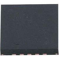
LTC4160EUDC-1#PBF Linear Technology, LTC4160EUDC-1#PBF Datasheet - Page 11

LTC4160EUDC-1#PBF
Manufacturer Part Number
LTC4160EUDC-1#PBF
Description
IC, BATT CHRG, Li-Ion, Li-Polymer, 1.2A, QFN20
Manufacturer
Linear Technology
Datasheet
1.LTC4160EUDC-1PBF.pdf
(32 pages)
Specifications of LTC4160EUDC-1#PBF
Battery Type
Li-Ion, Li-Polymer
Input Voltage
5.5V
Battery Charge Voltage
4.1V
Charge Current Max
1.2A
Battery Ic Case Style
QFN
No. Of Pins
20
No. Of Series Cells
1
Rohs Compliant
Yes
Lead Free Status / RoHS Status
Lead free / RoHS Compliant
Lead Free Status / RoHS Status
Lead free / RoHS Compliant
Available stocks
Company
Part Number
Manufacturer
Quantity
Price
PIN FUNCTIONS
V
via the SW pin by drawing controlled current from a DC
source such as a USB port or DC output wall adapter.
In On-The-Go mode this pin provides power to external
loads. Bypass V
ceramic capacitor.
SW (Pin 14): The SW pin transfers power between V
to V
the Applications Information section for a discussion of
inductance value and current rating.
I
input current limit of the bidirectional PowerPath switching
regulator in step-down mode. See Table 1. Each has an
internal 1.8µA pull-down current source.
CLPROG (Pin 17): USB Current Limit Program and Monitor
Pin. A 1% resistor from CLPROG to ground determines
the upper limit of the current drawn or sourced from the
V
is sent to the CLPROG pin when the PMOS switch of the
bidirectional PowerPath switching regulator is on. The
switching regulator delivers power until the CLPROG pin
reaches 1.18V in step-down mode and 1.15V in step-up
mode. When the switching regulator is in step-down mode,
CLPROG is used to regulate the average input current.
Several V
input which will typically correspond to the 500mA and
100mA USB specifications. When the switching regulator
is in step-up mode (USB On-The-Go), CLPROG is used to
limit the average output current to 680mA. A multilayer
ceramic averaging capacitor or R-C network is required
at CLPROG for filtering.
LIM0
BUS
BUS
OUT
, I
(Pin 13): Power Pin. This pin delivers power to V
pin. A precise fraction, h
LIM1
via the bidirectional switching regulator. See
BUS
(Pins 15, 16): I
current limit settings are available via user
BUS
with a low impedance multilayer
LIM0
CLPROG
and I
LIM1
, of the V
control the V
BUS
current
OUT
BUS
BUS
LDO3V3 (Pin 18): 3.3V LDO Output Pin. This pin provides
a regulated always-on 3.3V supply voltage. LDO3V3
gets its power from V
such as a watch dog microprocessor or real time clock.
A 1µF capacitor is required from LDO3V3 to ground. If
the LDO3V3 output is not used it should be disabled by
connecting it to V
NTCBIAS (Pin 19): NTC Thermistor Bias Output. If NTC
operation is desired, connect a bias resistor between
NTCBIAS and NTC, and an NTC thermistor between NTC
and GND. To disable NTC operation, connect NTC to GND
and leave NTCBIAS open.
NTC (Pin 20): Input to the Thermistor Monitoring Circuits.
The NTC pin connects to a negative temperature coefficient
thermistor, which is typically co-packaged with the battery,
to determine if the battery is too hot or too cold to charge.
If the battery’s temperature is out of range, charging is
paused until it re-enters the valid range. A low drift bias
resistor is required from NTCBIAS to NTC and a thermistor
is required from NTC to ground. To disable NTC operation,
connect NTC to GND and leave NTCBIAS open.
GND (Exposed Pad Pin 21): Ground. The Exposed Pad
should be connected to a continuous ground plane on the
second layer of the printed circuit board by several vias
directly under the LTC4160/LTC4160-1.
LTC4160/LTC4160-1
OUT
.
OUT
. It may be used for light loads
11
41601fa


