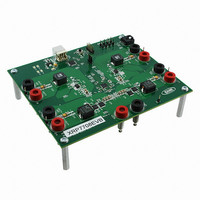
XRP7708EVB Exar Corporation, XRP7708EVB Datasheet - Page 7

XRP7708EVB
Manufacturer Part Number
XRP7708EVB
Description
EVAL BOARD FOR XRP7708
Manufacturer
Exar Corporation
Type
PMIC Solutionsr
Specifications of XRP7708EVB
Main Purpose
DC/DC, Step Down
Outputs And Type
*
Voltage - Output
*
Current - Output
*
Voltage - Input
*
Regulator Topology
Buck
Frequency - Switching
*
Board Type
Fully Populated
Utilized Ic / Part
XRP7708
Board Size
6 mm x 6 mm x 0.8 mm
Interface Type
I2C
Maximum Operating Temperature
+ 125 C
Operating Supply Voltage
6.5 V to 20 V
Product
Power Management Development Tools
Sense Voltage (max)
5 mV
Dimensions
6 mm x 6 mm x 0.8 mm
Silicon Manufacturer
Exar
Silicon Core Number
XRP7708
Kit Application Type
Power Management - Voltage Regulator
Application Sub Type
Step Down DC/DC Controller
For Use With/related Products
XRP7708
Lead Free Status / RoHS Status
Lead free / RoHS Compliant
Power - Output
-
Lead Free Status / RoHS Status
Lead free / RoHS Compliant
Other names
1016-1346
ORDERING INFORMATION
“YY” = Year – “WW” = Work Week – “X” = Lot Number
© 2010 Exar Corporation
XRP7708ILB- F
XRP7708ILBTR-F
XRP7708EVB
VOUT1-VOUT4
GPIO0-GPIO3
GPIO4_SDA,
Part Number
BST1-BST4
GPIO5_SCL
GH1-GH4
GL1-GL4
LDOOUT
LX1-LX4
ENABLE
Name
DVDD
AGND
AGND
DGND
Pin Number
Exposed Pad
XRP7708 Evaluation Board
17,22,30,55
19,24,28,33
34,29,23,18
32,27,20,25
12,13,14,15
Temperature Range
-40°C≤T
-40°C≤T
3,4,5,6
7,8
10
11
40
2
9
J
J
≤+125°C
≤+125°C
Input for powering the internal digital logic. This pin should be connected to AVDD.
Digital Ground. This pin should be connected to the ground plane at the exposed pad
with a separate trace.
Analog Ground. This pin should be connected to the ground plane at the exposed pad
with a separate trace
Output pin of the low side gate driver. Connect directly to the respective gate of an
external N-channel MOSFET.
Output pin of the high side gate driver. Connect directly to the respective gate of an
external N-channel MOSFET.
Lower supply rail for the high-side gate driver (GHx). Connect this pin to the switching
node at the junction between the two external power MOSFETs and the inductor. These
pins are also used to measure voltage drop across bottom MOSFETs in order to provide
output current information to the control engine.
High side driver supply pin(s). Connect BST to an external boost diode and a capacitor
as shown in the front page diagram.
The high side driver is connected between the BST pin and LX pin.
These pins can be configured as inputs or outputs to implement custom flags, power
good signals and enable/disable controls. A GPIO pin can also be programmed as an
input clock synchronizing IC to external clock. Refer to the “GPIO Pins” Section and the
“External Clock Synchronization” Section for more information.
I
GPIO functions in applications when I
Voltage sense.
Connect to the output of the corresponding power stage.
Output of the Standby LDO. It can be configured as a 5V or 3.3V output. A
compensation capacitor should be used on this pin [see Application Note].
If ENABLE is pulled high, the chip powers up (logic reset, registers configuration loaded,
etc.). If pulled low for longer than 100us, the XRP7708 is placed into shutdown.
Analog Ground.
Connect to analog ground (as noted above for pin 11).
2
C serial interface communication pins. These pins can be re-programmed to perform
Q
Q
XRP7708ILB
XRP7708ILB
Marking
YYWW X
YYWW X
u
u
a
a
d
d
C
C
h
h
40-pin TQFN
40-pin TQFN
a
a
Package
n
n
7/27
n
n
e
e
l
l
D
D
i
i
Packing Quantity
g
g
3K/Tape & Reel
i
i
2
Description
C bus is not used.
t
t
a
a
l
l
Bulk
P
P
W
W
M
M
S
S
Halogen Free
Halogen Free
t
t
e
e
p
p
Note 1
D
D
o
o
w
w
n
n
X
X
C
C
R
R
o
o
n
P
n
P
Rev. 1.0.3
Note 2
t
t
7
7
r
r
o
7
o
7
l
l
0
0
l
l
e
e
8
8
r
r


