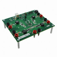
XRP7708EVB Exar Corporation, XRP7708EVB Datasheet
XRP7708EVB
Specifications of XRP7708EVB


Related parts for XRP7708EVB

XRP7708EVB Summary of contents
Page 1
... The device offers a complete solution for soft- start and soft-stop. The start-up delay and ramp of each PWM regulator independently controlled. The device can start up a pre-biased PWM channel without causing large negative inductor current. TYPICAL APPLICATION DIAGRAM Exar Corporation 48720 Kato Road, Fremont CA 94538, USA ...
Page 2
... Step Down Controllers Parameter VOUT Regulation Accuracy VOUT regulation range VOUT set point resolution VOUT set point resolution VOUT Input Current VOUT Input Resistance Load Current Note 1: Voltages above 5.1V can be obtained by using an external voltage divider. Low Drop-out Regulator © 2010 Exar Corporation ...
Page 3
... Input Pin High Level Input Pin Leakage Current Input pin Capacitance Output Pin Low Level Output Pin High Level Output Pin High Level (no load Specification Parameter Speed Input Pin Low Level Input Pin High Level Hysteresis of Schmitt Trigger Inputs, V HYS © 2010 Exar Corporation ...
Page 4
... IHMIN 20+0.1C V ILMAX Capacitance for each I/O Pin Note the capacitance one one bus Gate Drivers Parameter GH, GL Rise and Fall Time GH, GL Pull-up On-State Output Resistance GH, GL Pull-down On-State Output Resistance GH, GL Pull-down Off-State Output Resistance © 2010 Exar Corporation ...
Page 5
... BLOCK DIAGRAM © 2010 Exar Corporation Fig. 2: XRP7708 Block Diagram 5/ Rev. 1.0 ...
Page 6
... PIN ASSIGNMENT PIN DESCRIPTION Name Pin Number 39 VIN1 38 VIN2 37 VCCA 26 VCCD 36,31,16,21 PGND1- PGND4 1 AVDD © 2010 Exar Corporation Fig. 3: XRP7708 Pin Assignment Power source for the internal linear regulators to generate VCCA, VDD and the Standby LDO (LDOOUT). Place a decoupling capacitor close to the controller IC. Also used in UVLO1 fault generation – ...
Page 7
... AGND ORDERING INFORMATION Part Number Temperature Range XRP7708ILB- F -40°C≤T ≤+125°C J XRP7708ILBTR-F -40°C≤T ≤+125°C J XRP7708 Evaluation Board XRP7708EVB “YY” = Year – “WW” = Work Week – “X” = Lot Number © 2010 Exar Corporation ...
Page 8
... Fig. 4: 12Vin Efficiency: Single Channel 300kHz - Channels not in use are disabled FET: Si4944; Inductor: 744314xxx 7x7x5mm Fig. 6: 12Vin Efficiency: Single Channel 300kHz - Channels not in use are disabled FET: FDS8984; Inductor:744310200 7x7x3mm Fig. 8: Simultaneous Start-up Configuration CH1:3.3V CH2:5V CH3:1V CH4:1.8V © 2010 Exar Corporation ...
Page 9
... Fig. 10: Sequential Start-up Configuration CH1:3.3V CH2:5V CH3:1V CH4:1.8V Fig. 12: Startup into 3V prebias – 5V Output CH1: Vout(5V) Fig. 14: Load Transient Response CH1:Iout (1A/div) CH2: Vout (3.3V) © 2010 Exar Corporation Fig. 11: Sequential Soft-Stop Configuration CH1:5V CH2:3.3V CH3:1.8V CH4:1.2V Vout Shutdown = 0.8V, 3A load Fig ...
Page 10
... Fig. 15: Temperature Regulation 1.8V out (+/- 1% Vo window) © 2010 Exar Corporation Fig. 16: Temperature Regulation 1.0V out (+/- 1% Vo window) 10/ Rev. 1.0 ...
Page 11
... Fault reporting (including OCP, OVP, Temperature, Soft-Start in progress, Power Good) − Allows a Logic Level interface with other non-digital IC’ logic inputs to other devices − Possible to configure as traditional ‘enable’ pin for all 4 outputs © 2010 Exar Corporation ...
Page 12
... The figure below shows the power-up sequence of XRP7708 during the normal operation. The startup stage is divided into three phases. The first phase is the internal LDO power-up phase. The second phase is the configuration transfer phase. The third phase is chip ready phase. The power up sequence is less than 1ms. © 2010 Exar Corporation ...
Page 13
... For enabling a specific channel, there are several ways that this can be achieved. The chip can be configured to enable a channel at start-up as the default configuration residing in the non-volatile configuration memory of the IC. The channels can also be enabled using GPIO pins and/ © 2010 Exar Corporation Q u ...
Page 14
... VIN2 VIN2 is required to be tied to VIN1 pin. It can be used as a UVLO detection pin. If VIN2 falls below its user programmed limit, all channels are shut down. Temperature Monitoring and Over Temperature Protection (OTP) • Reading the junction temperature © 2010 Exar Corporation ...
Page 15
... The output voltage regulation in this case might exceed 2% due to extra error from the resistor divider. R1 and R2 follows the definition below. Fig. 18: External divider network for high output voltage © 2010 Exar Corporation ...
Page 16
... To calculate the maximum current limit, the user needs to provide the MOSFET Rdson. The maximum current can be calculated as: Where Kt is the temperature coefficient of the MOSFET Rdson; Vsense is the voltage across Rdson; IOUTMAX is the maximum output current. Over-Current Warning © 2010 Exar Corporation ...
Page 17
... Bits [15:10] specify the delay after disabling a channel but before starting the shutdown of the channel; where each bit represents 250us steps. Bits [9:0] specify the fall time of the channel; these 10 bits define the number of microseconds for each 50mV increment to reach the discharge threshold. © 2010 Exar Corporation ...
Page 18
... There are a number of options that could result in similar PWM switching frequency as shown above. In general, the chip consumes less power at lower oscillator frequency. When synchronization to external clock is needed, the user can choose the oscillator frequency to be © 2010 Exar Corporation ...
Page 19
... When the duty cycle limit is reached, the output voltage will no longer regulate and will be clamped based on the maximum duty cycle limit setting. Efficiency © 2010 Exar Corporation ...
Page 20
... Two XRP7708s can be synchronized together. This Master-Slave configuration is described below. • Master When the XRP7708 powers master unit after the internal configuration memory is loaded the unit will send CLK_OUT and SYNC_OUT signals to the slave on the preconfigured GPIO pins. • Slave © 2010 Exar Corporation ...
Page 21
... Master/Slave CLK_IN, or CLK_IN can go to the Master, and the Master can synchronize SYNC_OUT and CLK_OUT to the Slave. CLK_IN Fig. 24: External Clock Synchronization Master Slave Combination CLK_IN Fig. 25:Alternative External clock synchronization Master Slave combination © 2010 Exar Corporation ...
Page 22
... The GPIOs can be configured to signal Fault or Warning conditions when they occur in the chip. Each GPIO can be configured to signal one of the following: • OCP Fault on Channel • OCP Warning on Channel • OVP Fault on Channel • UVLO Fault on VIN1 or VIN2 • UVLO Warning on VIN1 or VIN2 • Over Temperature Fault or Warning © 2010 Exar Corporation ...
Page 23
... Use the following equation to calculate Cout: Where the output inductance I2 is the step load high current I1 is the step load low current Vos is output voltage including the overshoot Vout is the steady state output voltage Or it can be expressed approximately by © 2010 Exar Corporation ...
Page 24
... In general, the total input voltage ripple should be kept below 1.5% of VIN. The input voltage ripple also has two major components: the voltage drop on the main capacitor voltage drop due to ESR - calculated from: Total input voltage ripple is the sum of the above: © 2010 Exar Corporation ...
Page 25
... Selecting MOSFETs with lower Rdson reduces conduction losses at the expense of increased switching losses. A simplified expression for conduction losses is given by: MOSFET’s junction temperature can be estimated from: This assumes that the switching loss is the same as the conduction loss. thermal resistance from junction to ambient. © 2010 Exar Corporation ...
Page 26
... PACKAGE SPECIFICATION 40 TQFN IN MMX MM © 2010 Exar Corporation 26/ Rev. 1.0 ...
Page 27
... While the information in this publication has been carefully checked; no responsibility, however, is assumed for inaccuracies. EXAR Corporation does not recommend the use of any of its products in life support applications where the failure or malfunction of the product can reasonably be expected to cause failure of the life support system or to significantly affect its safety or effectiveness. Products are not authorized for use in such applications unless EXAR Corporation receives, in writing, assurances to its satisfaction that: (a) the risk of injury or damage has been minimized ...