EVAL-ADF4153EBZ1 Analog Devices Inc, EVAL-ADF4153EBZ1 Datasheet - Page 5
EVAL-ADF4153EBZ1
Manufacturer Part Number
EVAL-ADF4153EBZ1
Description
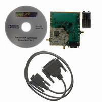
BOARD EVAL FOR ADF4153
Manufacturer
Analog Devices Inc
Datasheet
1.ADF4153BRUZ.pdf
(24 pages)
Specifications of EVAL-ADF4153EBZ1
Main Purpose
Timing, Frequency Synthesizer
Embedded
No
Utilized Ic / Part
ADF4153
Primary Attributes
Single Fractional-N PLL
Secondary Attributes
1.75GHz, Graphical User Interface
Lead Free Status / RoHS Status
Lead free / RoHS Compliant


Parameter
NOISE CHARACTERISTICS
1
2
3
4
5
6
7
8
TIMING SPECIFICATIONS
AV
dBm referred to 50 Ω.
Table 2.
Parameter
t
t
t
t
t
t
t
1
2
3
4
5
6
7
Operating temperature for B version is −40°C to +85°C.
Operating temperature for Y version is −40°C to +125°C.
AC coupling ensures AV
Guaranteed by design. Sample tested to ensure compliance.
The synthesizer phase noise floor is estimated by measuring the in-band phase noise at the output of the VCO and subtracting 20 log(N) (where N is the N divider
value) and 10 log(F
The PLL phase noise is composed of 1/f (flicker) noise plus the normalized PLL noise floor. The formula for calculating the 1/f noise contribution at an RF frequency, F
and at an offset frequency, f, is given by PN = P
The phase noise is measured with the EVAL-ADF4153EBZ1 and the Agilent E5500 phase noise system.
f
REFIN
Normalized Phase Noise Floor
Normalized 1/f Noise (PN
Phase Noise Performance
1750 MHz Output
DD
(PN
= 100 MHz; F
= DV
SYNTH
DD
)
5
= SDV
DATA
PFD
CLK
PFD
LE
LE
= 25 MHz; offset frequency = 5 kHz; RF
). PN
8
DD
DD
Limit at T
20
10
10
25
25
10
20
/2 bias.
SYNTH
= 2.7 V to 3.3 V; V
DB23 (MSB)
t
= PN
1
1_f
7
)
6
TOT
MIN
− 10 log(F
to T
B Version
−220
−114
−102
MAX
1_f
PFD
t
+ 10 log(10 kHz/f) + 20 log(F
2
P
(B Version)
) − 20 log(N).
= AV
DB22
1
DD
OUT
t
Y Version
−220
−114
−102
3
to 5.5 V; AGND = DGND = 0 V; T
= 1750 MHz; N = 70; loop BW = 20 kHz; lowest noise mode.
Figure 2. Timing Diagram
Rev. D | Page 5 of 24
2
DB2
RF
Unit
dBc/Hz typ
dBc/Hz typ
dBc/Hz typ
/1 GHz). Both the normalized phase noise floor and flicker noise are modeled in ADIsimPLL.
t
4
t
Unit
ns min
ns min
ns min
ns min
ns min
ns min
ns min
5
(CONTROL BIT C2)
Test Conditions/Comments
PLL loop BW = 500 kHz
Measured at 10 kHz offset, normalized to 1 GHz
@ VCO output
@ 5 kHz offset, 25 MHz PFD frequency
DB1
A
= T
MIN
Test Conditions/Comments
LE setup time
DATA to CLK setup time
DATA to CLK hold time
CLK high duration
CLK low duration
CLK to LE setup time
LE pulse width
to T
MAX
t
6
(CONTROL BIT C1)
, unless otherwise noted;
DB0 (LSB)
t
7
ADF4153
RF
,
Related parts for EVAL-ADF4153EBZ1
Image
Part Number
Description
Manufacturer
Datasheet
Request
R

Part Number:
Description:
IC, ADJ LDO REG, 1.5V TO 5V 250mA MSOP-8
Manufacturer:
Vishay
Datasheet:

Part Number:
Description:
IC, ADJ LDO REG, 1.5V TO 5V 0.6A 8-TSSOP
Manufacturer:
Vishay
Datasheet:
Part Number:
Description:
IC, ADJ LDO REG, 1.5V TO 5V 250mA MSOP-8
Manufacturer:
Vishay
Datasheet:

Part Number:
Description:
IC ADJ LDO REG 1.5V TO 5V 150mA 5-SOT-23
Manufacturer:
Vishay
Datasheet:

Part Number:
Description:
BOARD EVAL AS1324-AD
Manufacturer:
austriamicrosystems
Datasheet:
Part Number:
Description:
IC, ADJ LDO REG, 1.5V TO 5V 0.6A 8-TSSOP
Manufacturer:
Vishay
Datasheet:

Part Number:
Description:
IC, ADJ LDO REG, 1.5V TO 5V, 0.3A, MSOP8
Manufacturer:
Vishay
Datasheet:
Part Number:
Description:
IC, ADJ LDO REG, 1.5V TO 5V, 0.3A, MSOP8
Manufacturer:
Vishay
Datasheet:
Part Number:
Description:
IC, ADJ LDO REG 1.215V TO 5V 0.3A MSOP-8
Manufacturer:
Vishay
Datasheet:
Part Number:
Description:
IC, ADJ LDO REG 1.215V TO 5V 0.3A MSOP-8
Manufacturer:
Vishay
Datasheet:

Part Number:
Description:
±1.7g Dual-Axis IMEMS Accelerometer Evaluation Board
Manufacturer:
Analog Devices Inc
Datasheet:

Part Number:
Description:
IC MULTIPLIER ANALOG 8-SOIC T/R
Manufacturer:
Analog Devices Inc
Datasheet:

Part Number:
Description:
IC ANALOG MULTIPLIER 8-DIP
Manufacturer:
Analog Devices Inc
Datasheet:
Part Number:
Description:
IC ANALOG MULTIPLIER 8-SOIC
Manufacturer:
Analog Devices Inc
Datasheet:
Part Number:
Description:
IC ANALOG MULTIPLIER 8-DIP
Manufacturer:
Analog Devices Inc
Datasheet: