EVAL-ADF4153EBZ1 Analog Devices Inc, EVAL-ADF4153EBZ1 Datasheet - Page 2
EVAL-ADF4153EBZ1
Manufacturer Part Number
EVAL-ADF4153EBZ1
Description
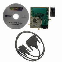
BOARD EVAL FOR ADF4153
Manufacturer
Analog Devices Inc
Datasheet
1.ADF4153BRUZ.pdf
(24 pages)
Specifications of EVAL-ADF4153EBZ1
Main Purpose
Timing, Frequency Synthesizer
Embedded
No
Utilized Ic / Part
ADF4153
Primary Attributes
Single Fractional-N PLL
Secondary Attributes
1.75GHz, Graphical User Interface
Lead Free Status / RoHS Status
Lead free / RoHS Compliant


ADF4153
TABLE OF CONTENTS
Features .............................................................................................. 1
Applications....................................................................................... 1
General Description ......................................................................... 1
Functional Block Diagram .............................................................. 1
Revision History ............................................................................... 2
Specifications..................................................................................... 4
Absolute Maximum Ratings............................................................ 6
Pin Configurations and Function Descriptions ........................... 7
Typical Performance Characteristics ............................................. 8
Circuit Description........................................................................... 9
REVISION HISTORY
8/10—Rev. C to Rev. D
Changes to Features Section............................................................ 1
Changes to Noise Characteristics Parameter, Table 1.................. 5
Changes to Figure 4.......................................................................... 7
Changes to Ordering Guide .......................................................... 24
Added Automotive Products Section .......................................... 24
10/08—Rev. B to Rev. C
Added Y Version (Throughout) ..................................................... 1
Changes to Ordering Guide .......................................................... 23
08/05—Rev. A to Rev. B
Changes to Features.......................................................................... 1
Changes to Applications .................................................................. 1
Changes to Specifications ................................................................ 3
Changes to Absolute Maximum Ratings ....................................... 5
Changes to Figure 7 to Figure 9 ...................................................... 7
Deleted Figure 8 to Figure 10; Renumbered Sequentially........... 8
Timing Specifications .................................................................. 5
ESD Caution.................................................................................. 6
Reference Input Section............................................................... 9
RF Input Stage............................................................................... 9
RF INT Divider............................................................................. 9
INT, FRAC, MOD, and R Relationship ..................................... 9
RF R Counter ................................................................................ 9
Phase Frequency Detector (PFD) and Charge Pump............ 10
MUXOUT and Lock Detect...................................................... 10
Input Shift Registers ................................................................... 10
Program Modes .......................................................................... 10
N Divider Register, R0 ............................................................... 16
Rev. D | Page 2 of 24
Applications Information .............................................................. 22
Outline Dimensions ....................................................................... 23
Deleted Figure 11 and Figure 14; Renumbered Sequentially ......9
Changes to Table 9.......................................................................... 13
Added Initialization Sequence Section........................................ 17
Changes to Fastlock with Spurious Optimization Section ....... 18
Inserted Figure 16; Renumbered Sequentially ........................... 18
Added Spur Mechanisms Section ................................................ 18
Added Table 11; Renumbered Sequentially ................................ 18
Added Spur Consistency Section ................................................. 19
Changes to Phase Resync Section ................................................ 19
Inserted Figure 17; Renumbered Sequentially ........................... 19
Deleted Spurious Signals—
Predicting Where They Will Appear Section ............................. 20
Changes to Figure 19...................................................................... 20
Changes to Figure 20...................................................................... 21
Added Applications Section.......................................................... 21
Changes to Figure 22 Caption ...................................................... 22
Changes to Ordering Guide .......................................................... 22
R Divider Register, R1................................................................ 16
Control Register, R2................................................................... 16
Noise and Spur Register, R3...................................................... 17
Reserved Bits............................................................................... 17
Initialization Sequence .............................................................. 18
RF Synthesizer: A Worked Example ........................................ 18
Modulus....................................................................................... 18
Reference Doubler and Reference Divider ............................. 18
12-Bit Programmable Modulus................................................ 18
Fastlock with Spurious Optimization...................................... 19
Spur Mechanisms ....................................................................... 19
Spur Consistency........................................................................ 20
Phase Resync............................................................................... 20
Filter Design—ADIsimPLL....................................................... 20
Interfacing ................................................................................... 20
PCB Design Guidelines for Chip Scale Package .................... 21
Local Oscillator for a GSM Base Station Transmitter ........... 22
Ordering Guide .......................................................................... 24
Automotive Products ................................................................. 24
Related parts for EVAL-ADF4153EBZ1
Image
Part Number
Description
Manufacturer
Datasheet
Request
R

Part Number:
Description:
IC, ADJ LDO REG, 1.5V TO 5V 250mA MSOP-8
Manufacturer:
Vishay
Datasheet:

Part Number:
Description:
IC, ADJ LDO REG, 1.5V TO 5V 0.6A 8-TSSOP
Manufacturer:
Vishay
Datasheet:
Part Number:
Description:
IC, ADJ LDO REG, 1.5V TO 5V 250mA MSOP-8
Manufacturer:
Vishay
Datasheet:

Part Number:
Description:
IC ADJ LDO REG 1.5V TO 5V 150mA 5-SOT-23
Manufacturer:
Vishay
Datasheet:

Part Number:
Description:
BOARD EVAL AS1324-AD
Manufacturer:
austriamicrosystems
Datasheet:
Part Number:
Description:
IC, ADJ LDO REG, 1.5V TO 5V 0.6A 8-TSSOP
Manufacturer:
Vishay
Datasheet:

Part Number:
Description:
IC, ADJ LDO REG, 1.5V TO 5V, 0.3A, MSOP8
Manufacturer:
Vishay
Datasheet:
Part Number:
Description:
IC, ADJ LDO REG, 1.5V TO 5V, 0.3A, MSOP8
Manufacturer:
Vishay
Datasheet:
Part Number:
Description:
IC, ADJ LDO REG 1.215V TO 5V 0.3A MSOP-8
Manufacturer:
Vishay
Datasheet:
Part Number:
Description:
IC, ADJ LDO REG 1.215V TO 5V 0.3A MSOP-8
Manufacturer:
Vishay
Datasheet:

Part Number:
Description:
±1.7g Dual-Axis IMEMS Accelerometer Evaluation Board
Manufacturer:
Analog Devices Inc
Datasheet:

Part Number:
Description:
IC MULTIPLIER ANALOG 8-SOIC T/R
Manufacturer:
Analog Devices Inc
Datasheet:

Part Number:
Description:
IC ANALOG MULTIPLIER 8-DIP
Manufacturer:
Analog Devices Inc
Datasheet:
Part Number:
Description:
IC ANALOG MULTIPLIER 8-SOIC
Manufacturer:
Analog Devices Inc
Datasheet:
Part Number:
Description:
IC ANALOG MULTIPLIER 8-DIP
Manufacturer:
Analog Devices Inc
Datasheet: