EVAL-ADF4153EBZ1 Analog Devices Inc, EVAL-ADF4153EBZ1 Datasheet - Page 21
EVAL-ADF4153EBZ1
Manufacturer Part Number
EVAL-ADF4153EBZ1
Description
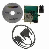
BOARD EVAL FOR ADF4153
Manufacturer
Analog Devices Inc
Datasheet
1.ADF4153BRUZ.pdf
(24 pages)
Specifications of EVAL-ADF4153EBZ1
Main Purpose
Timing, Frequency Synthesizer
Embedded
No
Utilized Ic / Part
ADF4153
Primary Attributes
Single Fractional-N PLL
Secondary Attributes
1.75GHz, Graphical User Interface
Lead Free Status / RoHS Status
Lead free / RoHS Compliant


When operating in this mode, the maximum SCLOCK rate of
the ADuC812 is 4 MHz. This means that the maximum rate at
which the output frequency can be changed is 180 kHz.
ADSP-21xx Interface
Figure 19 shows the interface between the ADF4153 and the
ADSP-21xx digital signal processor. As discussed previously,
the ADF4153 needs a 24-bit serial word for each latch write.
The easiest way to accomplish this using the ADSP-21xx family
is to use the autobuffered transmit mode of operation with
alternate framing. This provides a means for transmitting an
entire block of serial data before an interrupt is generated.
Set up the word length for eight bits and use three memory
locations for each 24-bit word. To program each 24-bit latch,
store the three 8-bit bytes, enable the autobuffered mode, and
write to the transmit register of the DSP. This last operation
initiates the autobuffer transfer.
ADSP-21xx
I/O FLAGS
Figure 19. ADSP-21xx to ADF4153 Interface
SCLK
TFS
DT
CLK
DATA
LE
MUXOUT
(LOCK DETECT)
ADF4153
Rev. D | Page 21 of 24
PCB DESIGN GUIDELINES FOR CHIP SCALE
PACKAGE
The lands on the chip scale package (CP-20) are rectangular.
The printed circuit board (PCB) pad for these should be 0.1 mm
longer than the package land length and 0.05 mm wider than
the package land width. The land should be centered on the
pad. This ensures that the solder joint size is maximized.
The bottom of the chip scale package has a central thermal pad.
The thermal pad on the PCB should be at least as large as this
exposed pad. On the PCB, there should be a clearance of at least
0.25 mm between the thermal pad and the inner edges of the
pad pattern. This ensures that shorting is avoided.
Thermal vias can be used on the PCB thermal pad to improve
thermal performance of the package. If vias are used, they should
be incorporated in the thermal pad at 1.2 mm pitch grid. The
via diameter should be between 0.3 mm and 0.33 mm, and the
via barrel should be plated with one ounce of copper to plug the
via. The user should connect the PDB thermal pad to AGND.
ADF4153
Related parts for EVAL-ADF4153EBZ1
Image
Part Number
Description
Manufacturer
Datasheet
Request
R

Part Number:
Description:
IC, ADJ LDO REG, 1.5V TO 5V 250mA MSOP-8
Manufacturer:
Vishay
Datasheet:

Part Number:
Description:
IC, ADJ LDO REG, 1.5V TO 5V 0.6A 8-TSSOP
Manufacturer:
Vishay
Datasheet:
Part Number:
Description:
IC, ADJ LDO REG, 1.5V TO 5V 250mA MSOP-8
Manufacturer:
Vishay
Datasheet:

Part Number:
Description:
IC ADJ LDO REG 1.5V TO 5V 150mA 5-SOT-23
Manufacturer:
Vishay
Datasheet:

Part Number:
Description:
BOARD EVAL AS1324-AD
Manufacturer:
austriamicrosystems
Datasheet:
Part Number:
Description:
IC, ADJ LDO REG, 1.5V TO 5V 0.6A 8-TSSOP
Manufacturer:
Vishay
Datasheet:

Part Number:
Description:
IC, ADJ LDO REG, 1.5V TO 5V, 0.3A, MSOP8
Manufacturer:
Vishay
Datasheet:
Part Number:
Description:
IC, ADJ LDO REG, 1.5V TO 5V, 0.3A, MSOP8
Manufacturer:
Vishay
Datasheet:
Part Number:
Description:
IC, ADJ LDO REG 1.215V TO 5V 0.3A MSOP-8
Manufacturer:
Vishay
Datasheet:
Part Number:
Description:
IC, ADJ LDO REG 1.215V TO 5V 0.3A MSOP-8
Manufacturer:
Vishay
Datasheet:

Part Number:
Description:
±1.7g Dual-Axis IMEMS Accelerometer Evaluation Board
Manufacturer:
Analog Devices Inc
Datasheet:

Part Number:
Description:
IC MULTIPLIER ANALOG 8-SOIC T/R
Manufacturer:
Analog Devices Inc
Datasheet:

Part Number:
Description:
IC ANALOG MULTIPLIER 8-DIP
Manufacturer:
Analog Devices Inc
Datasheet:
Part Number:
Description:
IC ANALOG MULTIPLIER 8-SOIC
Manufacturer:
Analog Devices Inc
Datasheet:
Part Number:
Description:
IC ANALOG MULTIPLIER 8-DIP
Manufacturer:
Analog Devices Inc
Datasheet: