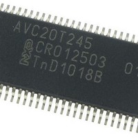
74AVC20T245DGG,118 NXP Semiconductors, 74AVC20T245DGG,118 Datasheet - Page 13

74AVC20T245DGG,118
Manufacturer Part Number
74AVC20T245DGG,118
Description
TXRX 20BIT TRANSLAT 56TSSOP
Manufacturer
NXP Semiconductors
Datasheet
1.74AVC20T245DGV118.pdf
(27 pages)
Specifications of 74AVC20T245DGG,118
Logic Family
74AVC
Number Of Channels Per Chip
2
Propagation Delay Time
6 ns, 11.8 ns
Supply Voltage (max)
3.6 V
Supply Voltage (min)
0.8 V
Maximum Operating Temperature
+ 125 C
Package / Case
TSSOP-56
Maximum Power Dissipation
600 mW
Minimum Operating Temperature
- 40 C
Mounting Style
SMD/SMT
Lead Free Status / RoHS Status
Lead free / RoHS Compliant
Other names
568-5250-2
NXP Semiconductors
Table 12.
Voltages are referenced to GND (ground = 0 V); for test circuit see
[1]
74AVC20T245
Product data sheet
Symbol Parameter
V
t
t
t
V
t
t
t
V
t
t
t
V
t
t
t
V
t
t
t
pd
dis
en
pd
dis
en
pd
dis
en
pd
dis
en
pd
dis
en
CC(A)
CC(A)
CC(A)
CC(A)
CC(A)
t
pd
is the same as t
= 1.1 V to 1.3 V
= 1.4 V to 1.6 V
= 1.65 V to 1.95 V
= 2.3 V to 2.7 V
= 3.0 V to 3.6 V
propagation
delay
disable time
enable time
propagation
delay
disable time
enable time
propagation
delay
disable time
enable time
propagation
delay
disable time
enable time
propagation
delay
disable time
enable time
Dynamic characteristics for temperature range 40 C to +85 C
PLH
and t
Conditions
nAn to nBn
nBn to nAn
nOE to nAn
nOE to nBn
nOE to nAn
nOE to nBn
nAn to nBn
nBn to nAn
nOE to nAn
nOE to nBn
nOE to nAn
nOE to nBn
nAn to nBn
nBn to nAn
nOE to nAn
nOE to nBn
nOE to nAn
nOE to nBn
nAn to nBn
nBn to nAn
nOE to nAn
nOE to nBn
nOE to nAn
nOE to nBn
nAn to nBn
nBn to nAn
nOE to nAn
nOE to nBn
nOE to nAn
nOE to nBn
PHL
; t
dis
is the same as t
1.2 V 0.1 V
Min
0.5
0.5
2.0
1.5
1.5
1.0
0.5
0.5
2.0
1.5
1.5
1.0
0.5
0.5
2.0
1.5
1.0
0.5
0.5
0.5
1.1
1.2
0.5
0.5
0.5
0.5
0.8
1.2
0.5
1.0
All information provided in this document is subject to legal disclaimers.
Max
11.9
12.7
15.3
15.6
11.7
10.3
14.3
11.3
13.8
10.8
13.3
10.5
13.1
9.0
7.4
8.1
5.2
5.4
5.0
4.4
Rev. 4 — 24 November 2010
9.4
9.4
8.9
7.1
8.7
6.2
8.4
5.2
8.2
5.1
PLZ
and t
1.5 V 0.1 V 1.8 V 0.15 V 2.5 V 0.2 V
Min
0.5
0.5
1.5
1.0
0.5
0.5
2.0
1.5
1.0
0.5
0.5
2.0
1.0
0.5
0.5
0.5
1.1
0.5
0.5
0.5
0.8
0.5
2.0
1.5
1.5
1.5
1.2
0.5
1.2
1.0
PHZ
; t
en
Max
11.9
15.3
11.5
10.3
10.3
10.0
7.1
8.9
9.8
6.4
6.4
9.0
9.0
6.1
5.4
7.4
8.7
8.1
5.8
4.3
5.2
8.2
5.4
9.6
5.7
3.9
5.0
8.1
4.4
9.6
is the same as t
20-bit dual supply translating transceiver; 3-state
Figure
Min
0.5
0.5
2.0
1.5
1.5
1.0
0.5
0.5
2.0
1.5
1.5
1.0
0.5
0.5
2.0
1.5
1.0
0.5
0.5
0.5
1.1
1.2
0.5
0.5
0.5
0.5
0.8
1.2
0.5
0.5
7; for wave forms see
V
CC(B)
PZL
10.0
Max
11.9
15.3
10.3
[1]
6.2
8.7
9.6
5.4
6.1
9.0
7.8
8.4
5.0
5.0
7.4
7.4
7.9
7.9
4.7
3.9
5.2
6.9
5.3
7.6
4.6
3.5
5.0
6.7
4.3
7.5
and t
PZH
Min
0.5
0.5
2.0
1.0
1.5
0.5
0.5
0.5
2.0
1.0
1.5
0.5
0.5
0.5
2.0
1.0
1.0
0.5
0.5
0.5
1.1
1.0
0.5
0.5
0.5
0.5
0.8
1.0
0.5
0.5
.
74AVC20T245
Max
15.3
10.2
Figure 5
11.9
5.2
8.4
8.1
8.4
4.3
5.8
9.0
6.4
6.1
3.9
4.7
7.4
5.8
7.9
5.7
3.5
3.5
5.2
5.3
5.2
5.3
3.4
3.0
5.0
5.1
4.2
5.1
3.3 V 0.3 V
© NXP B.V. 2010. All rights reserved.
Min
0.5
0.5
2.0
1.0
1.5
0.5
0.5
0.5
2.0
1.0
1.5
0.5
0.5
0.5
2.0
1.0
1.0
0.5
0.5
0.5
1.1
1.0
0.5
0.5
0.5
0.5
0.8
0.8
0.5
0.5
and
Figure
Max
15.3
10.2
11.9
5.1
8.2
9.0
8.0
3.9
5.7
9.0
6.0
5.3
3.5
4.6
7.4
5.6
7.9
4.8
3.0
3.4
5.2
5.2
5.2
4.3
2.9
2.9
5.0
5.0
4.1
4.1
6.
13 of 27
Unit
ns
ns
ns
ns
ns
ns
ns
ns
ns
ns
ns
ns
ns
ns
ns
ns
ns
ns
ns
ns
ns
ns
ns
ns
ns
ns
ns
ns
ns
ns


