74AVC16T245DGG,118 NXP Semiconductors, 74AVC16T245DGG,118 Datasheet - Page 15
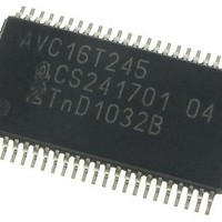
74AVC16T245DGG,118
Manufacturer Part Number
74AVC16T245DGG,118
Description
TXRX 16BIT TRANSLAT 48TSSOP
Manufacturer
NXP Semiconductors
Datasheet
1.74AVC16T245DGV118.pdf
(28 pages)
Specifications of 74AVC16T245DGG,118
Logic Family
74AVC
Number Of Channels Per Chip
2
Propagation Delay Time
6 ns, 11.8 ns
Supply Voltage (max)
3.6 V
Supply Voltage (min)
0.8 V
Maximum Operating Temperature
+ 125 C
Package / Case
TSSOP-48
Maximum Power Dissipation
500 mW
Minimum Operating Temperature
- 40 C
Mounting Style
SMD/SMT
Lead Free Status / RoHS Status
Lead free / RoHS Compliant
Other names
568-5248-2


NXP Semiconductors
11. Waveforms
Table 14.
[1]
[2]
74AVC16T245_2
Product data sheet
Supply voltage
V
0.8 V to 1.6 V
1.65 V to 2.7 V
3.0 V to 3.6 V
Fig 6.
Fig 7.
CC(A)
V
V
CCI
CCO
, V
is the supply voltage associated with the data input port.
CC(B)
is the supply voltage associated with the output port.
Measurement points are given in
V
The data input (nAn, nBn) to output (nBn, nAn) propagation delay times
Measurement points are given in
V
Enable and disable times
OL
OL
Measurement points
and V
and V
OH
OH
are typical output voltage levels that occur with the output load.
are typical output voltage levels that occur with the output load.
HIGH-to-OFF
OFF-to-HIGH
Input
V
0.5V
0.5V
0.5V
LOW-to-OFF
OFF-to-LOW
nOE input
M
output
output
CCI
CCI
CCI
[1]
nBn, nAn output
nAn, nBn input
V
GND
GND
V
Table
CCO
Table
V
OH
OL
V
All information provided in this document is subject to legal disclaimers.
I
GND
14.
14.
V
V
OH
OL
V
I
Rev. 02 — 30 March 2010
V
M
enabled
Output
V
0.5V
0.5V
0.5V
t
outputs
PLZ
t
PHZ
M
CCO
CCO
CCO
V
[2]
V
M
X
V
V
Y
M
t
PHL
16-bit dual supply translating transceiver; 3-state
disabled
outputs
V
V
V
V
X
OL
OL
OL
t
PZL
t
PZH
+ 0.1 V
+ 0.15 V
+ 0.3 V
001aak285
t
PLH
V
M
V
001aak286
M
outputs
enabled
74AVC16T245
V
V
V
V
Y
OH
OH
OH
© NXP B.V. 2010. All rights reserved.
− 0.1 V
− 0.15 V
− 0.3 V
15 of 28
Related parts for 74AVC16T245DGG,118
Image
Part Number
Description
Manufacturer
Datasheet
Request
R

Part Number:
Description:
NXP Semiconductors designed the LPC2420/2460 microcontroller around a 16-bit/32-bitARM7TDMI-S CPU core with real-time debug interfaces that include both JTAG andembedded trace
Manufacturer:
NXP Semiconductors
Datasheet:

Part Number:
Description:
NXP Semiconductors designed the LPC2458 microcontroller around a 16-bit/32-bitARM7TDMI-S CPU core with real-time debug interfaces that include both JTAG andembedded trace
Manufacturer:
NXP Semiconductors
Datasheet:
Part Number:
Description:
NXP Semiconductors designed the LPC2468 microcontroller around a 16-bit/32-bitARM7TDMI-S CPU core with real-time debug interfaces that include both JTAG andembedded trace
Manufacturer:
NXP Semiconductors
Datasheet:
Part Number:
Description:
NXP Semiconductors designed the LPC2470 microcontroller, powered by theARM7TDMI-S core, to be a highly integrated microcontroller for a wide range ofapplications that require advanced communications and high quality graphic displays
Manufacturer:
NXP Semiconductors
Datasheet:
Part Number:
Description:
NXP Semiconductors designed the LPC2478 microcontroller, powered by theARM7TDMI-S core, to be a highly integrated microcontroller for a wide range ofapplications that require advanced communications and high quality graphic displays
Manufacturer:
NXP Semiconductors
Datasheet:
Part Number:
Description:
The Philips Semiconductors XA (eXtended Architecture) family of 16-bit single-chip microcontrollers is powerful enough to easily handle the requirements of high performance embedded applications, yet inexpensive enough to compete in the market for hi
Manufacturer:
NXP Semiconductors
Datasheet:
Part Number:
Description:
The XA-S3 device is a member of Philips Semiconductors? XA(eXtended Architecture) family of high performance 16-bitsingle-chip microcontrollers
Manufacturer:
NXP Semiconductors
Datasheet:

Part Number:
Description:
The NXP BlueStreak LH75401/LH75411 family consists of two low-cost 16/32-bit System-on-Chip (SoC) devices
Manufacturer:
NXP Semiconductors
Datasheet:
Part Number:
Description:
The NXP LPC3130/3131 combine an 180 MHz ARM926EJ-S CPU core, high-speed USB2
Manufacturer:
NXP Semiconductors
Datasheet:
Part Number:
Description:
The NXP LPC3141 combine a 270 MHz ARM926EJ-S CPU core, High-speed USB 2
Manufacturer:
NXP Semiconductors
Part Number:
Description:
The NXP LPC3143 combine a 270 MHz ARM926EJ-S CPU core, High-speed USB 2
Manufacturer:
NXP Semiconductors

Part Number:
Description:
The NXP LPC3152 combines an 180 MHz ARM926EJ-S CPU core, High-speed USB 2
Manufacturer:
NXP Semiconductors
Part Number:
Description:
The NXP LPC3154 combines an 180 MHz ARM926EJ-S CPU core, High-speed USB 2
Manufacturer:
NXP Semiconductors

Part Number:
Description:
Standard level N-channel enhancement mode Field-Effect Transistor (FET) in a plastic package using NXP High-Performance Automotive (HPA) TrenchMOS technology
Manufacturer:
NXP Semiconductors
Datasheet: