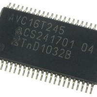
74AVC16T245DGG,118 NXP Semiconductors, 74AVC16T245DGG,118 Datasheet
74AVC16T245DGG,118
Specifications of 74AVC16T245DGG,118


Related parts for 74AVC16T245DGG,118


74AVC16T245DGG,118 Summary of contents
Page 1
Rev. 02 — 30 March 2010 1. General description The 74AVC16T245 is a 16-bit transceiver with bidirectional level voltage translation and 3-state outputs.The device can be used as two ...
Page 2
... NXP Semiconductors 100 Mbit/s (≥ 1 1.2 V translation) Suspend mode Latch-up performance exceeds 100 mA per JESD 78 Class II Inputs accept voltages OFF Multiple package options Specified from −40 °C to +85 °C and −40 °C to +125 °C 3. Ordering information Table 1. Ordering information Type number ...
Page 3
... NXP Semiconductors V V CC(A) CC(B) 1OE 1DIR V V CC(A) CC(B) 2OE 2DIR Fig 2. Logic symbol 74AVC16T245_2 Product data sheet 16-bit dual supply translating transceiver; 3-state 1B1 1B2 1B3 1A1 1A2 1A3 1A4 2B1 2B2 2B3 2A1 2A2 2A3 2A4 All information provided in this document is subject to legal disclaimers. ...
Page 4
... NXP Semiconductors 5. Pinning information 5.1 Pinning 74AVC16T245 1DIR 1 1B1 2 3 1B2 4 GND 1B3 5 1B4 CC(B) 8 1B5 9 1B6 GND 10 1B7 11 1B8 12 13 2B1 14 2B2 GND 15 2B3 16 2B4 CC(B) 19 2B5 2B6 20 GND 21 2B7 22 23 2B8 24 2DIR Fig 3. Pin configuration SOT362-1 and SOT480-1 (TSSOP48) ...
Page 5
... NXP Semiconductors terminal 1 index area (1) The die substrate is attached to this pad using conductive die attach material. It can not be used as a supply pin or input. Fig 5. Pin configuration SOT1134-1 (HXQFN60U) 74AVC16T245_2 Product data sheet 16-bit dual supply translating transceiver; 3-state D1 A32 A31 A30 ...
Page 6
... NXP Semiconductors 5.2 Pin description Table 2. Pin description Symbol Pin SOT362-1 and SOT480-1 1DIR, 2DIR 1, 24 1B1 to 1B8 11, 12 2B1 to 2B8 13, 14, 16, 17, 19, 20, 22, 23 [1] GND 4, 10, 15, 21, 28, 34, 39 CC(B) 1OE, 2OE 48, 25 1A1 to 1A8 47, 46, 44, 43, 41, 40, 38, 37 2A1 to 2A8 ...
Page 7
... NXP Semiconductors 7. Limiting values Table 4. Limiting values In accordance with the Absolute Maximum Rating System (IEC 60134). Voltages are referenced to GND (ground = 0 V). Symbol Parameter V supply voltage A CC(A) V supply voltage B CC(B) I input clamping current IK V input voltage I I output clamping current OK V output voltage ...
Page 8
... NXP Semiconductors 9. Static characteristics Table 6. Typical static characteristics recommended operating conditions; voltages are referenced to GND (ground = 0 V). Symbol Parameter V HIGH-level output voltage OH V LOW-level output voltage OL I input leakage current I I OFF-state output current OZ I power-off leakage current OFF C input capacitance ...
Page 9
... NXP Semiconductors Table 7. Static characteristics At recommended operating conditions; voltages are referenced to GND (ground = 0 V). Symbol Parameter Conditions V LOW-level data input IL input voltage V CCI V CCI V CCI V CCI nDIR, nOE input V CC(A) V CC(A) V CC(A) V CC(A) V HIGH-level output voltage = −100 μ CC(A) = −3 mA; ...
Page 10
... NXP Semiconductors Table 7. Static characteristics At recommended operating conditions; voltages are referenced to GND (ground = 0 V). Symbol Parameter Conditions I power-off A port; V OFF leakage V CC(A) current B port CC(B) I supply current A port CC(A) V CC(B) V CC(A) V CC(B) V CC(A) V CC(A) B port CC(A) V CC(B) V CC(A) V CC(B) V CC(A) V CC(A) ...
Page 11
... NXP Semiconductors 10. Dynamic characteristics Table 9. Typical power dissipation capacitance at V Voltages are referenced to GND (ground = 0 V). Symbol Parameter Conditions C power dissipation A port: (direction nAn to PD capacitance nBn); output enabled A port: (direction nAn to nBn); output disabled A port: (direction nBn to nAn); output enabled A port: (direction nBn to nAn) ...
Page 12
... NXP Semiconductors Table 10. Typical dynamic characteristics at V Voltages are referenced to GND (ground = 0 V); for test circuit see Symbol Parameter Conditions t propagation delay nAn to nBn pd nBn to nAn t disable time nOE to nAn dis nOE to nBn t enable time nOE to nAn en nOE to nBn [ the same as t and t ...
Page 13
... NXP Semiconductors Dynamic characteristics for temperature range −40 °C to +85 °C Table 12. Voltages are referenced to GND (ground = 0 V); for test circuit see Symbol Parameter Conditions 1.3 V CC(A) t propagation nAn to nBn pd delay nBn to nAn t disable time nOE to nAn dis nOE to nBn ...
Page 14
... NXP Semiconductors Dynamic characteristics for temperature range −40 °C to +125 °C Table 13. Voltages are referenced to GND (ground = 0 V); for test circuit see Symbol Parameter Conditions 1.3 V CC(A) t propagation nAn to nBn pd delay nBn to nAn t disable time nOE to nAn dis nOE to nBn ...
Page 15
... NXP Semiconductors 11. Waveforms Measurement points are given in V and V are typical output voltage levels that occur with the output load Fig 6. The data input (nAn, nBn) to output (nBn, nAn) propagation delay times nOE input output LOW-to-OFF OFF-to-LOW output HIGH-to-OFF OFF-to-HIGH Measurement points are given in ...
Page 16
... NXP Semiconductors Test data is given in Table R = Load resistance Load capacitance including jig and probe capacitance Termination resistance External voltage for measuring switching times. EXT Fig 8. Load circuit for switching times Table 15. Test data Supply voltage Input [ CC(A) CC( CCI 1. 2.7 V ...
Page 17
... NXP Semiconductors 12. Typical propagation delay characteristics (ns Propagation delay (nAn to nBn 0.8 V. CC(B) ( 1.2 V. CC(B) ( 1.5 V. CC(B) ( 1.8 V. CC(B) ( 2.5 V. CC(B) ( 3.3 V. CC(B) Fig 9. Typical propagation delay versus load capacitance; T 74AVC16T245_2 Product data sheet 16-bit dual supply translating transceiver; 3-state 001aai476 t pd ...
Page 18
... NXP Semiconductors 7 t PLH (ns LOW to HIGH propagation delay (nAn to nBn 1.2 V CC( PLH (ns LOW to HIGH propagation delay (nAn to nBn 1.5 V CC(A) ( 1.2 V. CC(B) ( 1.5 V. CC(B) ( 1.8 V. CC(B) ( 2.5 V. CC(B) ( 3.3 V. CC(B) Fig 10. Typical propagation delay versus load capacitance; T 74AVC16T245_2 Product data sheet 16-bit dual supply translating transceiver ...
Page 19
... NXP Semiconductors 7 t PLH (ns LOW to HIGH propagation delay (nAn to nBn 1.8 V CC( PLH (ns LOW to HIGH propagation delay (nAn to nBn 2.5 V CC(A) ( 1.2 V. CC(B) ( 1.5 V. CC(B) ( 1.8 V. CC(B) ( 2.5 V. CC(B) ( 3.3 V. CC(B) Fig 11. Typical propagation delay versus load capacitance; T 74AVC16T245_2 Product data sheet 16-bit dual supply translating transceiver ...
Page 20
... NXP Semiconductors 7 t PLH (ns LOW to HIGH propagation delay (nAn to nBn 3.3 V CC(A) ( 1.2 V. CC(B) ( 1.5 V. CC(B) ( 1.8 V. CC(B) ( 2.5 V. CC(B) ( 3.3 V. CC(B) Fig 12. Typical propagation delay versus load capacitance; T 74AVC16T245_2 Product data sheet 16-bit dual supply translating transceiver; 3-state 001aai485 t PHL ...
Page 21
... NXP Semiconductors 13. Package outline TSSOP48: plastic thin shrink small outline package; 48 leads; body width 6 pin 1 index 1 DIMENSIONS (mm are the original dimensions). A UNIT max. 0.15 1.05 mm 1.2 0.25 0.05 0.85 Notes 1. Plastic or metal protrusions of 0.15 mm maximum per side are not included. 2. Plastic interlead protrusions of 0.25 mm maximum per side are not included. ...
Page 22
... NXP Semiconductors TSSOP48: plastic thin shrink small outline package; 48 leads; body width 4.4 mm; lead pitch 0 pin 1 index 1 DIMENSIONS (mm are the original dimensions) A UNIT max. 0.15 0.95 mm 1.1 0.25 0.05 0.85 Notes 1. Plastic or metal protrusions of 0.15 mm maximum per side are not included. ...
Page 23
... NXP Semiconductors VFBGA56: plastic very thin fine-pitch ball grid array package; 56 balls; body 4 0.65 mm ball A1 index area ball A1 1 index area DIMENSIONS (mm are the original dimensions) A UNIT max. 0.3 0.7 0. 0.2 0.6 0.35 OUTLINE VERSION IEC SOT702-1 Fig 15. Package outline SOT702-1 (VFBGA56) ...
Page 24
... NXP Semiconductors HXQFN60U: plastic thermal enhanced extremely thin quad flat package; no leads; 60 terminals; UTLP based; body 0.5 mm terminal 1 index area A10 terminal 1 index area D1 Dimensions Unit max 0.50 0.05 0.35 4.1 mm nom 0.48 0.02 0.30 4.0 min 0.46 0.00 0.25 3.9 ...
Page 25
... NXP Semiconductors 14. Abbreviations Table 16. Abbreviations Acronym Description CDM Charged Device Model DUT Device Under Test ESD ElectroStatic Discharge HBM Human Body Model MM Machine Model 15. Revision history Table 17. Revision history Document ID Release date 74AVC16T245_2 20100330 • Modifications: 74AVC16T245BQ changed from HUQFN60U (SOT1025-1) to HXQFN60U (SOT1134-1) package ...
Page 26
... In no event shall NXP Semiconductors be liable for any indirect, incidental, punitive, special or consequential damages (including - without limitation - lost profits, lost savings, business interruption, costs related to the removal or ...
Page 27
... NXP Semiconductors 17. Contact information For more information, please visit: For sales office addresses, please send an email to: 74AVC16T245_2 Product data sheet 16-bit dual supply translating transceiver; 3-state http://www.nxp.com salesaddresses@nxp.com All information provided in this document is subject to legal disclaimers. Rev. 02 — 30 March 2010 74AVC16T245 © ...
Page 28
... NXP Semiconductors 18. Contents 1 General description . . . . . . . . . . . . . . . . . . . . . . 1 2 Features and benefits . . . . . . . . . . . . . . . . . . . . 1 3 Ordering information . . . . . . . . . . . . . . . . . . . . . 2 4 Functional diagram . . . . . . . . . . . . . . . . . . . . . . 2 5 Pinning information . . . . . . . . . . . . . . . . . . . . . . 4 5.1 Pinning . . . . . . . . . . . . . . . . . . . . . . . . . . . . . . . 4 5.2 Pin description . . . . . . . . . . . . . . . . . . . . . . . . . 6 6 Functional description . . . . . . . . . . . . . . . . . . . 6 7 Limiting values Recommended operating conditions Static characteristics Dynamic characteristics . . . . . . . . . . . . . . . . . 11 11 Waveforms . . . . . . . . . . . . . . . . . . . . . . . . . . . . 15 12 Typical propagation delay characteristics . . 17 13 Package outline ...