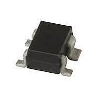
BFG25AW/X,115 NXP Semiconductors, BFG25AW/X,115 Datasheet - Page 6

BFG25AW/X,115
Manufacturer Part Number
BFG25AW/X,115
Description
TRANS RF NPN 5GHZ 5V SOT343
Manufacturer
NXP Semiconductors
Datasheet
1.BFG25AWX115.pdf
(14 pages)
Specifications of BFG25AW/X,115
Package / Case
SOT-343N
Transistor Type
NPN
Voltage - Collector Emitter Breakdown (max)
5V
Frequency - Transition
5GHz
Noise Figure (db Typ @ F)
1.9dB ~ 2dB @1GHz
Power - Max
500mW
Dc Current Gain (hfe) (min) @ Ic, Vce
50 @ 500µA, 1V
Current - Collector (ic) (max)
6.5mA
Mounting Type
Surface Mount
Dc Collector/base Gain Hfe Min
50
Dc Current Gain Hfe Max
200
Mounting Style
SMD/SMT
Configuration
Single
Transistor Polarity
NPN
Collector- Emitter Voltage Vceo Max
5 V
Emitter- Base Voltage Vebo
2 V
Continuous Collector Current
6.5 mA
Power Dissipation
500 mW
Lead Free Status / RoHS Status
Lead free / RoHS Compliant
Gain
-
Lead Free Status / RoHS Status
Lead free / RoHS Compliant, Lead free / RoHS Compliant
Other names
568-6185-2
BFG25AW/X,115
BFG25AW/X,115
NXP Semiconductors
1998 Sep 23
handbook, halfpage
handbook, full pagewidth
NPN 5 GHz wideband transistors
V
f = 500 MHz; V
CE
(dB)
= 1 V.
F
Fig.10 Minimum noise figure as a function
4
3
2
1
0
10
−1
CE
of collector current; typical values.
= 1 V; I
C
= 1 mA; Z
1
180
Fig.12 Common emitter noise figure circles; typical values.
o
= 50
o
1 GHz
500 MHz
f = 2 GHz
I C (mA)
0
135
135
0.2
0.2
o
o
0.2
MCD145
0.5
0.5
10
0.5
6
90
90
1
1
1
o
o
handbook, halfpage
V
F = 5 dB
CE
(dB)
= 1 V.
Fig.11 Minimum noise figure as a function of
F
2
F = 4 dB
4
3
2
1
0
10
F
2
min
F = 3 dB
2
2
frequency; typical values.
= 1.9 dB
5
BFG25AW; BFG25AW/X
45
Γ
45
opt
o
o
5
5
MLB977
0
o
10
3
1.0
0.8
0.6
0.4
0.2
0
1.0
I C = 2 mA
1 mA
0.5 mA
f (MHz)
Product specification
MCD146
10
4


