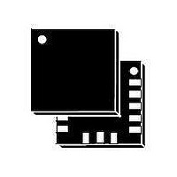
L3G4200D STMicroelectronics, L3G4200D Datasheet - Page 24

L3G4200D
Manufacturer Part Number
L3G4200D
Description
Gyroscopes Mems Sensor 3-Axis 2.4 to 3.6 V Gyro
Manufacturer
STMicroelectronics
Datasheet
1.L3G4200D.pdf
(29 pages)
Specifications of L3G4200D
Sensing Axis
Triple
Supply Current
6.1 mA
Digital Output - Number Of Bits
16 bit
Maximum Operating Temperature
+ 85 C
Minimum Operating Temperature
- 40 C
Supply Voltage (max)
3.6 V
Supply Voltage (min)
2.4 V
Sensitivity
70 mV/deg/s
Output Type
Digital
Package / Case
LGA-16
No. Of Axes
3
Interface Type
I2C, SPI
Sensitivity Per Axis
70mdps / Digit
Sensor Case Style
LGA
No. Of Pins
16
Supply Voltage Range
2.4V To 3.6V
Operating Temperature Range
-40°C To +85°C
Rohs Compliant
Yes
Lead Free Status / RoHS Status
Lead free / RoHS Compliant
Available stocks
Company
Part Number
Manufacturer
Quantity
Price
Company:
Part Number:
L3G4200D
Manufacturer:
STMicroelectronics
Quantity:
1 400
Part Number:
L3G4200D
Manufacturer:
ST
Quantity:
20 000
Part Number:
L3G4200DTR
Manufacturer:
ST
Quantity:
20 000
Digital interfaces
5.2.2
24/29
The SPI read command is performed with 16 clock pulses. A multiple byte read command is
performed by adding blocks of 8 clock pulses to the previous one.
Bit 0: READ bit. The value is 1.
Bit 1: MS bit. When 0, do not increment address; when 1, increment address in multiple
reading.
Bit 2-7: address AD(5:0). This is the address field of the indexed register.
Bit 8-15: data DO(7:0) (read mode). This is the data that is read from the device (MSb first).
Bit 16-... : data DO(...-8). Further data in multiple byte reading.
Figure 15. Multiple byte SPI read protocol (2-byte example)
SPI write
Figure 16. SPI write protocol
The SPI write command is performed with 16 clock pulses. A multiple byte write command is
performed by adding blocks of 8 clock pulses to the previous one.
Bit 0: WRITE bit. The value is 0.
Bit 1: MS bit. When 0, do not increment address; when 1, increment address in multiple
writing.
Bit 2 -7: address AD(5:0). This is the address field of the indexed register.
Bit 8-15: data DI(7:0) (write mode). This is the data that is written to the device (MSb first).
Bit 16-... : data DI(...-8). Further data in multiple byte writing.
SDO
SPC
SDI
CS
SPC
SDI
CS
RW
MS
AD5 AD4 AD3 AD2 AD1 AD0
RW
MS
AD5 AD4 AD3 AD2 AD1 AD0
Doc ID 17116 Rev 2
DO7 DO6 DO5 DO4 DO3 DO2 DO1 DO0
DI7 DI6 DI5 DI4 DI3 DI2 DI1 DI0
DO15 DO14 DO13 DO12 DO11 DO10 DO9 DO8
L3G4200D


