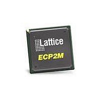
LFE2M35E-5FN484C Lattice, LFE2M35E-5FN484C Datasheet - Page 92

LFE2M35E-5FN484C
Manufacturer Part Number
LFE2M35E-5FN484C
Description
FPGA - Field Programmable Gate Array 34K LUTs SERDES MEM DSP 1.2V -5 Spd
Manufacturer
Lattice
Datasheet
1.LFE2-12SE-6FN256C.pdf
(389 pages)
Specifications of LFE2M35E-5FN484C
Number Of Macrocells
34000
Maximum Operating Frequency
311 MHz
Number Of Programmable I/os
303
Data Ram Size
2151424
Supply Voltage (max)
1.26 V
Maximum Operating Temperature
+ 85 C
Minimum Operating Temperature
0 C
Mounting Style
SMD/SMT
Supply Voltage (min)
1.14 V
Package / Case
FPBGA-484
Lead Free Status / RoHS Status
Lead free / RoHS Compliant
Available stocks
Company
Part Number
Manufacturer
Quantity
Price
Company:
Part Number:
LFE2M35E-5FN484C
Manufacturer:
Lattice
Quantity:
135
Company:
Part Number:
LFE2M35E-5FN484C
Manufacturer:
Lattice Semiconductor Corporation
Quantity:
10 000
- Current page: 92 of 389
- Download datasheet (5Mb)
Lattice Semiconductor
Figure 3-12. Transmitter and Receiver Block Diagram
HDOUTPi
HDOUTNi
HDINPi
HDINNi
Transmitter
Receiver
REFCLK
EQ
TX PLL
SERDES
REFCLK
CDR
Serializer
8:1/10:1
Transmit Clock
T4
Deserializer
R1
1:8/1:10
SERDES Bridge
R2
BYPASS
Polarity
Adjust
BYPASS
Polarity
Adjust
T3
Recovered Clock
3-40
BYPASS
R3
WA
Encoder
BYPASS
BYPASS
DEC
PCS
T2
DC and Switching Characteristics
LatticeECP2/M Family Data Sheet
R4
BYPASS
Elastic
Buffer
FIFO
R5
FPGA Bridge
Sample
Down
FIFO
Sample
R6
FIFO
Up
BYPASS
T1
FPGA Core
FPGA
EBRD Clock
Receive Data
FPGA
Receive Clock
Transmit Data
FPGA
Transmit Clock
Related parts for LFE2M35E-5FN484C
Image
Part Number
Description
Manufacturer
Datasheet
Request
R
Part Number:
Description:
IC, LATTICEECP2M FPGA, 420MHZ, FPBGA-672
Manufacturer:
LATTICE SEMICONDUCTOR
Datasheet:
Part Number:
Description:
IC, LATTICEECP2M FPGA, 420MHZ, FPBGA-256
Manufacturer:
LATTICE SEMICONDUCTOR
Datasheet:

Part Number:
Description:
FPGA - Field Programmable Gate Array 34K LUTs SERDES MEM DSP 1.2V -5 Spd
Manufacturer:
Lattice

Part Number:
Description:
FPGA - Field Programmable Gate Array 34K LUTs SERD Mem DS P 1.2V -5 Spd ES
Manufacturer:
Lattice

Part Number:
Description:
FPGA - Field Programmable Gate Array 34K LUTs SERDES MEM DSP 1.2V -6 Spd
Manufacturer:
Lattice
Datasheet:
Part Number:
Description:
FPGA LatticeECP2M Family 34000 Cells 90nm (CMOS) Technology 1.2V 484-Pin FBGA
Manufacturer:
LATTICE SEMICONDUCTOR
Datasheet:
Part Number:
Description:
FPGA LatticeECP2M Family 34000 Cells 90nm (CMOS) Technology 1.2V 484-Pin FBGA
Manufacturer:
LATTICE SEMICONDUCTOR
Datasheet:
Part Number:
Description:
FPGA LatticeECP2M Family 34000 Cells 90nm (CMOS) Technology 1.2V 256-Pin FBGA
Manufacturer:
LATTICE SEMICONDUCTOR
Datasheet:
Part Number:
Description:
FPGA LatticeECP2M Family 34000 Cells 90nm (CMOS) Technology 1.2V 484-Pin FBGA
Manufacturer:
LATTICE SEMICONDUCTOR
Datasheet:
Part Number:
Description:
FPGA LatticeECP2M Family 34000 Cells 90nm (CMOS) Technology 1.2V 484-Pin FBGA
Manufacturer:
LATTICE SEMICONDUCTOR
Datasheet:

Part Number:
Description:
IC FPGA 35KLUTS 410I/O 672-BGA
Manufacturer:
Lattice
Datasheet:

Part Number:
Description:
IC FPGA 35KLUTS 140I/O 256-BGA
Manufacturer:
Lattice
Datasheet:

Part Number:
Description:
IC FPGA 35KLUTS 140I/O 256-BGA
Manufacturer:
Lattice
Datasheet:

Part Number:
Description:
IC FPGA 35KLUTS 140I/O 256-BGA
Manufacturer:
Lattice
Datasheet:

Part Number:
Description:
IC FPGA 35KLUTS 140I/O 256-BGA
Manufacturer:
Lattice
Datasheet:


