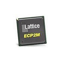
LFE2M35E-5FN484C Lattice, LFE2M35E-5FN484C Datasheet - Page 63

LFE2M35E-5FN484C
Manufacturer Part Number
LFE2M35E-5FN484C
Description
FPGA - Field Programmable Gate Array 34K LUTs SERDES MEM DSP 1.2V -5 Spd
Manufacturer
Lattice
Datasheet
1.LFE2-12SE-6FN256C.pdf
(389 pages)
Specifications of LFE2M35E-5FN484C
Number Of Macrocells
34000
Maximum Operating Frequency
311 MHz
Number Of Programmable I/os
303
Data Ram Size
2151424
Supply Voltage (max)
1.26 V
Maximum Operating Temperature
+ 85 C
Minimum Operating Temperature
0 C
Mounting Style
SMD/SMT
Supply Voltage (min)
1.14 V
Package / Case
FPBGA-484
Lead Free Status / RoHS Status
Lead free / RoHS Compliant
Available stocks
Company
Part Number
Manufacturer
Quantity
Price
Company:
Part Number:
LFE2M35E-5FN484C
Manufacturer:
Lattice
Quantity:
135
Company:
Part Number:
LFE2M35E-5FN484C
Manufacturer:
Lattice Semiconductor Corporation
Quantity:
10 000
- Current page: 63 of 389
- Download datasheet (5Mb)
Lattice Semiconductor
sysI/O Differential Electrical Characteristics
LVDS
Differential HSTL and SSTL
Differential HSTL and SSTL outputs are implemented as a pair of complementary single-ended outputs. All allow-
able single-ended output classes (class I and class II) are supported in this mode.
For further information about LVPECL, RSDS, MLVDS, BLVDS and other differential interfaces please see the list
of additional technical information at the end of this data sheet.
V
V
V
I
V
V
V
ýV
V
ýV
I
I
Parameter
IN
SA
SAB
OH
OL
OD
OS
INP
CM
THD
OD
OS
, V
INM
Input Voltage
Input Common Mode Voltage
Differential Input Threshold
Input Current
Output High Voltage for V
Output Low Voltage for V
Output Voltage Differential
Change in V
Low
Output Voltage Offset
Change in V
Output Short Circuit Current
Output Short Circuit Current
Description
OD
OS
Between H and L
Between High and
Over Recommended Operating Conditions
OP
OP
or V
or V
OM
OM
Half the Sum of the Two Inputs
Power On or Power Off
R
R
(V
(V
V
Ground
V
Each Other
Difference Between the Two Inputs
OD
OD
T
T
OP
OP
= 100 Ohm
= 100 Ohm
= 0V Driver Outputs Shorted to
= 0V Driver Outputs Shorted to
- V
+ V
OM
OM
3-11
Test Conditions
), R
)/2, R
T
= 100 Ohm
T
= 100 Ohm
DC and Switching Characteristics
LatticeECP2/M Family Data Sheet
+/-100
1.125
0.9V
Min.
0.05
250
—
—
—
—
—
—
0
Typ.
1.38
1.03
1.20
350
—
—
—
—
—
—
—
—
1.375
Max.
+/-10
2.35
1.60
450
2.4
50
50
24
12
—
—
Units
mV
mV
mV
mV
mA
mA
µA
V
V
V
V
V
Related parts for LFE2M35E-5FN484C
Image
Part Number
Description
Manufacturer
Datasheet
Request
R
Part Number:
Description:
IC, LATTICEECP2M FPGA, 420MHZ, FPBGA-672
Manufacturer:
LATTICE SEMICONDUCTOR
Datasheet:
Part Number:
Description:
IC, LATTICEECP2M FPGA, 420MHZ, FPBGA-256
Manufacturer:
LATTICE SEMICONDUCTOR
Datasheet:

Part Number:
Description:
FPGA - Field Programmable Gate Array 34K LUTs SERDES MEM DSP 1.2V -5 Spd
Manufacturer:
Lattice

Part Number:
Description:
FPGA - Field Programmable Gate Array 34K LUTs SERD Mem DS P 1.2V -5 Spd ES
Manufacturer:
Lattice

Part Number:
Description:
FPGA - Field Programmable Gate Array 34K LUTs SERDES MEM DSP 1.2V -6 Spd
Manufacturer:
Lattice
Datasheet:
Part Number:
Description:
FPGA LatticeECP2M Family 34000 Cells 90nm (CMOS) Technology 1.2V 484-Pin FBGA
Manufacturer:
LATTICE SEMICONDUCTOR
Datasheet:
Part Number:
Description:
FPGA LatticeECP2M Family 34000 Cells 90nm (CMOS) Technology 1.2V 484-Pin FBGA
Manufacturer:
LATTICE SEMICONDUCTOR
Datasheet:
Part Number:
Description:
FPGA LatticeECP2M Family 34000 Cells 90nm (CMOS) Technology 1.2V 256-Pin FBGA
Manufacturer:
LATTICE SEMICONDUCTOR
Datasheet:
Part Number:
Description:
FPGA LatticeECP2M Family 34000 Cells 90nm (CMOS) Technology 1.2V 484-Pin FBGA
Manufacturer:
LATTICE SEMICONDUCTOR
Datasheet:
Part Number:
Description:
FPGA LatticeECP2M Family 34000 Cells 90nm (CMOS) Technology 1.2V 484-Pin FBGA
Manufacturer:
LATTICE SEMICONDUCTOR
Datasheet:

Part Number:
Description:
IC FPGA 35KLUTS 410I/O 672-BGA
Manufacturer:
Lattice
Datasheet:

Part Number:
Description:
IC FPGA 35KLUTS 140I/O 256-BGA
Manufacturer:
Lattice
Datasheet:

Part Number:
Description:
IC FPGA 35KLUTS 140I/O 256-BGA
Manufacturer:
Lattice
Datasheet:

Part Number:
Description:
IC FPGA 35KLUTS 140I/O 256-BGA
Manufacturer:
Lattice
Datasheet:

Part Number:
Description:
IC FPGA 35KLUTS 140I/O 256-BGA
Manufacturer:
Lattice
Datasheet:


