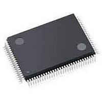
APA150-TQG100 Actel, APA150-TQG100 Datasheet - Page 30

APA150-TQG100
Manufacturer Part Number
APA150-TQG100
Description
FPGA - Field Programmable Gate Array 150K System Gates
Manufacturer
Actel
Datasheet
1.APA075-FGG144.pdf
(178 pages)
Specifications of APA150-TQG100
Processor Series
APA150
Core
IP Core
Maximum Operating Frequency
150 MHz
Number Of Programmable I/os
242
Data Ram Size
36864
Supply Voltage (max)
2.7 V
Maximum Operating Temperature
+ 70 C
Minimum Operating Temperature
0 C
Development Tools By Supplier
APA-Eval-Kit, APA-Eval-BRD1, Silicon-Explorer II, Silicon-Sculptor 3, SI-EX-TCA, Flashpro 4, Flashpro 3, Flashpro Lite
Mounting Style
SMD/SMT
Supply Voltage (min)
2.3 V
Number Of Gates
150 K
Package / Case
TQFP-100
Lead Free Status / RoHS Status
Lead free / RoHS Compliant
Available stocks
Company
Part Number
Manufacturer
Quantity
Price
Company:
Part Number:
APA150-TQG100A
Manufacturer:
Microsemi SoC
Quantity:
10 000
Company:
Part Number:
APA150-TQG100I
Manufacturer:
LT
Quantity:
1 400
Company:
Part Number:
APA150-TQG100I
Manufacturer:
Microsemi SoC
Quantity:
10 000
®
User Security
ProASIC
once programmed, block the entire programmed
contents from being read externally. Refer to
for details on the number of bits in the key for each
device. If locked, the user can only reprogram the device
employing the user-defined security key. This protects
the device from being read back and duplicated. Since
programmed data is stored in nonvolatile memory cells
(actually very small capacitors) rather than in the wiring,
physical deconstruction cannot be used to compromise
data. This type of security breach is further discouraged
by the placement of the memory cells beneath the four
metal layers (whose removal cannot be accomplished
without disturbing the charge in the capacitor). This is
the highest security provided in the industry. For more
information,
Nonvolatile Flash and Antifuse FPGAs
Table 2-11 • Flashlock Key Size by Device
Embedded Memory Floorplan
The embedded memory is located across the top and
bottom of the device in 256x9 blocks
1-2). Depending on the device, up to 88 blocks are
available to support a variety of memory configurations.
Each block can be programmed as an independent
memory array or combined (using dedicated memory
routing resources) to form larger, more complex memory
configurations. A single memory configuration could
include blocks from both the top and bottom memory
locations.
Table 2-12 • ProASIC
2 -2 0
Device
APA075
APA150
APA300
APA450
APA600
APA750
APA1000
Device
APA075
APA150
APA300
APA450
APA600
APA750
APA1000
ProASIC
PLUS
PLUS
devices have FlashLock protection bits that,
Flash Family FPGAs
refer
PLUS
Bottom
to
Memory Configurations by Device
16
24
28
32
44
0
0
Actel’s
Key Size
119 bits
167 bits
191 bits
263 bits
Design
79 bits
79 bits
79 bits
(Figure 1-1 on page
white paper.
Top
12
16
16
24
28
32
44
Security
Table 2-11
in
v5.9
256
256
256
256
256
256
256
D
Maximum Width
Embedded Memory Configurations
The embedded memory in the ProASIC
provides great configuration flexibility
ProASIC
port memory (one read, one write). This provides 198
kbits of two-port and/or single port memory in the
APA1000 device.
Each memory block can be configured as FIFO or SRAM,
with
asynchronous
Additional characteristics include programmable flags as
well as parity checking and generation.
page 2-22
diagrams of the basic SRAM and FIFO blocks.
on page 2-22
memory block SRAM and FIFO interface signals,
respectively. A single memory block is designed to
operate at up to 150 MHz (standard speed grade typical
conditions). Each block is comprised of 256 9-bit words
(one read port, one write port). The memory blocks may
be cascaded in width and/or depth to create the desired
memory organization.
provides optimal bit widths of 9 (one block), 18, 36, and
72, and optimal depths of 256, 512, 768, and 1,024. Refer
to Actel’s
Figure 2-21 on page 2-24
memory usage. Ten blocks with 23,040 bits have been
used to generate three arrays of various widths and
depths.
can be used in parallel to create extra read ports. In this
example, using only 10 of the 88 available blocks of the
APA1000 yields an effective 6,912 bits of multiple port
RAM. The Actel SmartGen software facilitates building
wider and deeper memory configurations for optimal
memory usage.
independent
PLUS
Figure 2-22 on page 2-24
SmartGen User’s Guide
and
block is designed and optimized as a two-
108
144
144
216
252
288
396
W
Figure 2-19 on page 2-23
and
read
Table 2-15 on page 2-23
selection
and
(Figure 2-20 on page
gives an example of optimal
1,536
2,048
2,048
3,072
3,584
4,096
5,632
write
D
Maximum Depth
for more information.
shows how RAM blocks
of
ports
(Table
synchronous
show the block
Figure 2-18 on
(Table
PLUS
2-12). Each
2-24). This
Table 2-14
W
9
9
9
9
9
9
9
describe
family
2-13).
or


