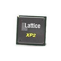
LFXP20C-3FN256C Lattice, LFXP20C-3FN256C Datasheet - Page 387

LFXP20C-3FN256C
Manufacturer Part Number
LFXP20C-3FN256C
Description
FPGA - Field Programmable Gate Array 19.7K LUTS 188 I/O
Manufacturer
Lattice
Specifications of LFXP20C-3FN256C
Number Of Programmable I/os
188
Data Ram Size
405504
Supply Voltage (max)
3.465 V
Maximum Operating Temperature
+ 90 C
Minimum Operating Temperature
0 C
Mounting Style
SMD/SMT
Supply Voltage (min)
1.71 V
Package / Case
FPBGA-256
Lead Free Status / RoHS Status
Lead free / RoHS Compliant
Available stocks
Company
Part Number
Manufacturer
Quantity
Price
Company:
Part Number:
LFXP20C-3FN256C
Manufacturer:
Lattice
Quantity:
135
Company:
Part Number:
LFXP20C-3FN256C
Manufacturer:
Lattice Semiconductor Corporation
Quantity:
10 000
- Current page: 387 of 397
- Download datasheet (10Mb)
Lattice Semiconductor
256-ball caBGA BGA Breakout Examples
This BGA breakout and routing example places a MachXO PLD in a 14x14 mm, 0.8 mm pitch, 256-ball caBGA
package (LCMXO2280-B256/BN256) into two fabrication scenarios. One for a 6-layer stack up with maximum I/O
utilization and a 4-layer with about 10% fewer I/Os. The 6-layer design (Example #1), demonstrates the best use of
mechanically drill blind vias to place caps near power pins to minimize layers.
Figure 14-10. CAM Artwork Screen Shots, Example #1, 256-Ball caBGA
Layer 1 Primary
Layer 5 Signal
Layer 3 GND
14-12
Layer 6 Secondary
PCB Layout Recommendations
Layer 2 Signal
Layer 4 Power
for BGA Packages
Related parts for LFXP20C-3FN256C
Image
Part Number
Description
Manufacturer
Datasheet
Request
R

Part Number:
Description:
FPGA - Field Programmable Gate Array 19.7K LUTs 340 IO 1. 8/2.5/3.3V -3 Spd I
Manufacturer:
Lattice

Part Number:
Description:
FPGA - Field Programmable Gate Array 19.7K LUTs 268 IO 1. 8/2.5/3.3V -3 Spd
Manufacturer:
Lattice

Part Number:
Description:
FPGA - Field Programmable Gate Array 19.7K LUTs 340 I/O 1.8/2.5/3.3V -3 Spd
Manufacturer:
Lattice
Datasheet:

Part Number:
Description:
FPGA - Field Programmable Gate Array 19.7K LUTs 268 IO 1. 8/2.5/3.3V -3 Spd I
Manufacturer:
Lattice
Part Number:
Description:
FPGA LatticeXP Family 20000 Cells 320MHz 130nm (CMOS) Technology 1.8V/2.5V/3.3V 256-Pin FBGA Tray
Manufacturer:
LATTICE SEMICONDUCTOR
Datasheet:
Part Number:
Description:
FPGA LatticeXP Family 20000 Cells 320MHz 130nm (CMOS) Technology 1.8V/2.5V/3.3V 388-Pin FBGA Tray
Manufacturer:
LATTICE SEMICONDUCTOR
Datasheet:
Part Number:
Description:
FPGA LatticeXP Family 20000 Cells 360MHz 130nm (CMOS) Technology 1.8V/2.5V/3.3V 256-Pin FBGA Tray
Manufacturer:
LATTICE SEMICONDUCTOR
Datasheet:
Part Number:
Description:
FPGA LatticeXP Family 20000 Cells 360MHz 130nm (CMOS) Technology 1.8V/2.5V/3.3V 388-Pin FBGA Tray
Manufacturer:
LATTICE SEMICONDUCTOR
Datasheet:
Part Number:
Description:
FPGA LatticeXP Family 20000 Cells 400MHz 130nm (CMOS) Technology 1.8V/2.5V/3.3V 256-Pin FBGA Tray
Manufacturer:
LATTICE SEMICONDUCTOR
Datasheet:
Part Number:
Description:
FPGA LatticeXP Family 20000 Cells 400MHz 130nm (CMOS) Technology 1.8V/2.5V/3.3V 256-Pin FBGA Tray
Manufacturer:
LATTICE SEMICONDUCTOR
Datasheet:

Part Number:
Description:
IC FPGA 19.7KLUTS 188I/O 256-BGA
Manufacturer:
Lattice
Datasheet:

Part Number:
Description:
IC FPGA 19.7KLUTS 340I/O 484-BGA
Manufacturer:
Lattice
Datasheet:

Part Number:
Description:
IC FPGA 19.7KLUTS 188I/O 256-BGA
Manufacturer:
Lattice
Datasheet:

Part Number:
Description:
IC FPGA 19.7KLUTS 188I/O 256-BGA
Manufacturer:
Lattice
Datasheet:


