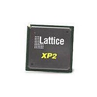
LFXP20C-3FN256C Lattice, LFXP20C-3FN256C Datasheet - Page 349

LFXP20C-3FN256C
Manufacturer Part Number
LFXP20C-3FN256C
Description
FPGA - Field Programmable Gate Array 19.7K LUTS 188 I/O
Manufacturer
Lattice
Specifications of LFXP20C-3FN256C
Number Of Programmable I/os
188
Data Ram Size
405504
Supply Voltage (max)
3.465 V
Maximum Operating Temperature
+ 90 C
Minimum Operating Temperature
0 C
Mounting Style
SMD/SMT
Supply Voltage (min)
1.71 V
Package / Case
FPBGA-256
Lead Free Status / RoHS Status
Lead free / RoHS Compliant
Available stocks
Company
Part Number
Manufacturer
Quantity
Price
Company:
Part Number:
LFXP20C-3FN256C
Manufacturer:
Lattice
Quantity:
135
Company:
Part Number:
LFXP20C-3FN256C
Manufacturer:
Lattice Semiconductor Corporation
Quantity:
10 000
- Current page: 349 of 397
- Download datasheet (10Mb)
Lattice Semiconductor
The above information was specified under the following environmental conditions:
The goal of this exercise is to compute the following device I/O constraints:
The only parameter which can be obtained from the above is the device junction temperature:
The required constraints can be computed as follows:
1. Input setup specification
2. Input hold specification
3. Output maximum propagation delay requirement
4. Output minimum propagation delay requirement
5. Output loading
The preference file to use for this example is shown in Figure 17-3. For more preference language syntax and
examples, refer to the Constraints & Preferences section of the ispLEVER on-line help system.
• Board trace AC loading (Cbac): 60 pf.
• Board trace parasitic capacitance (Cb): 5 pf.
• Port controller input capacitance (Cp) :9 pf.
• FPGA device input capacitance (Co): 9 pf.
• Maximum ambient temperature (Ta): 70 (C.
• Estimated Power Consumption (Q): 2 W.
• 680 PBGAM Package Thermal resistance (j) at 0 feet per minute (fpm) airflow: 13.4 °C/W.
1. Input setup specification.
2. Input hold specification.
3. Maximum output propagation delay.
4. Minimum output propagation delay.
5. Output loading.
6. Temperature.
Tj = j * Q - Ta
= 13.4 * 2 + 70
= 96.8 °C
= P - PDMAXp - PDMAXb - Tskew
= 30 - 18 - 2 - 1
= 9 ns
= PDMINp + PDMINb - Tskew
= 3 + 1 - 1
= 3 ns
= P - TSp - PDMAXb - Tskew
= 30 - 5 - 6 - 1
= 18 ns
= Thp - PDMINb + Tskew
= 3 - 1 + 1
= 3 ns
= Cbac + Cb + Cp
= 60 + 5 + 9
= 74 pf
17-5
Lattice Semiconductor FPGA
Successful Place and Route
Related parts for LFXP20C-3FN256C
Image
Part Number
Description
Manufacturer
Datasheet
Request
R

Part Number:
Description:
FPGA - Field Programmable Gate Array 19.7K LUTs 340 IO 1. 8/2.5/3.3V -3 Spd I
Manufacturer:
Lattice

Part Number:
Description:
FPGA - Field Programmable Gate Array 19.7K LUTs 268 IO 1. 8/2.5/3.3V -3 Spd
Manufacturer:
Lattice

Part Number:
Description:
FPGA - Field Programmable Gate Array 19.7K LUTs 340 I/O 1.8/2.5/3.3V -3 Spd
Manufacturer:
Lattice
Datasheet:

Part Number:
Description:
FPGA - Field Programmable Gate Array 19.7K LUTs 268 IO 1. 8/2.5/3.3V -3 Spd I
Manufacturer:
Lattice
Part Number:
Description:
FPGA LatticeXP Family 20000 Cells 320MHz 130nm (CMOS) Technology 1.8V/2.5V/3.3V 256-Pin FBGA Tray
Manufacturer:
LATTICE SEMICONDUCTOR
Datasheet:
Part Number:
Description:
FPGA LatticeXP Family 20000 Cells 320MHz 130nm (CMOS) Technology 1.8V/2.5V/3.3V 388-Pin FBGA Tray
Manufacturer:
LATTICE SEMICONDUCTOR
Datasheet:
Part Number:
Description:
FPGA LatticeXP Family 20000 Cells 360MHz 130nm (CMOS) Technology 1.8V/2.5V/3.3V 256-Pin FBGA Tray
Manufacturer:
LATTICE SEMICONDUCTOR
Datasheet:
Part Number:
Description:
FPGA LatticeXP Family 20000 Cells 360MHz 130nm (CMOS) Technology 1.8V/2.5V/3.3V 388-Pin FBGA Tray
Manufacturer:
LATTICE SEMICONDUCTOR
Datasheet:
Part Number:
Description:
FPGA LatticeXP Family 20000 Cells 400MHz 130nm (CMOS) Technology 1.8V/2.5V/3.3V 256-Pin FBGA Tray
Manufacturer:
LATTICE SEMICONDUCTOR
Datasheet:
Part Number:
Description:
FPGA LatticeXP Family 20000 Cells 400MHz 130nm (CMOS) Technology 1.8V/2.5V/3.3V 256-Pin FBGA Tray
Manufacturer:
LATTICE SEMICONDUCTOR
Datasheet:

Part Number:
Description:
IC FPGA 19.7KLUTS 188I/O 256-BGA
Manufacturer:
Lattice
Datasheet:

Part Number:
Description:
IC FPGA 19.7KLUTS 340I/O 484-BGA
Manufacturer:
Lattice
Datasheet:

Part Number:
Description:
IC FPGA 19.7KLUTS 188I/O 256-BGA
Manufacturer:
Lattice
Datasheet:

Part Number:
Description:
IC FPGA 19.7KLUTS 188I/O 256-BGA
Manufacturer:
Lattice
Datasheet:


