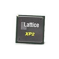
LFXP20C-3FN256C Lattice, LFXP20C-3FN256C Datasheet - Page 344

LFXP20C-3FN256C
Manufacturer Part Number
LFXP20C-3FN256C
Description
FPGA - Field Programmable Gate Array 19.7K LUTS 188 I/O
Manufacturer
Lattice
Specifications of LFXP20C-3FN256C
Number Of Programmable I/os
188
Data Ram Size
405504
Supply Voltage (max)
3.465 V
Maximum Operating Temperature
+ 90 C
Minimum Operating Temperature
0 C
Mounting Style
SMD/SMT
Supply Voltage (min)
1.71 V
Package / Case
FPBGA-256
Lead Free Status / RoHS Status
Lead free / RoHS Compliant
Available stocks
Company
Part Number
Manufacturer
Quantity
Price
Company:
Part Number:
LFXP20C-3FN256C
Manufacturer:
Lattice
Quantity:
135
Company:
Part Number:
LFXP20C-3FN256C
Manufacturer:
Lattice Semiconductor Corporation
Quantity:
10 000
- Current page: 344 of 397
- Download datasheet (10Mb)
Lattice Semiconductor
In the Synplicity
value to 1000 instead of using the default value of 100. This will guide the tool to allow high fanout signals without
replicating the logic. In the LeonardoSpectrum tool project GUI, under Technology => Advanced Settings, users
can set the Max Fanout to be any number instead of the default value “0”.
Use ispLEVER Project Navigator Results for Device Utilization and Performance
Many synthesis tools give usage reports at the end of a successful synthesis. These reports show the name and
the number of library elements used in the design. The data in these reports do not represent the actual implemen-
tation of the design in the final Place and Route tool because the EDIF netlist will be further optimized during Map-
ping and Place and Route to achieve the best results. It is strongly recommended to use the MAP report and the
PAR report in the ispLEVER Project Navigator tool to understand the actual resource utilization in the device.
Although the synthesis report also provides a performance summary, the timing information is based on estimated
logic delays only. The Place & Route TRACE Report in the ispLEVER Project Navigator gives accurate perfor-
mance analysis of the design by including actual logic and routing delays in the paths.
Technical Support Assistance
Hotline: 1-800-LATTICE (North America)
e-mail:
Internet:
+1-503-268-8001 (Outside North America)
techsupport@latticesemi.com
www.latticesemi.com
®
project GUI, under the Implementation Options => Devices tab, users can set the Fanout Guide
13-17
HDL Synthesis Coding Guidelines
for Lattice Semiconductor FPGAs
Related parts for LFXP20C-3FN256C
Image
Part Number
Description
Manufacturer
Datasheet
Request
R

Part Number:
Description:
FPGA - Field Programmable Gate Array 19.7K LUTs 340 IO 1. 8/2.5/3.3V -3 Spd I
Manufacturer:
Lattice

Part Number:
Description:
FPGA - Field Programmable Gate Array 19.7K LUTs 268 IO 1. 8/2.5/3.3V -3 Spd
Manufacturer:
Lattice

Part Number:
Description:
FPGA - Field Programmable Gate Array 19.7K LUTs 340 I/O 1.8/2.5/3.3V -3 Spd
Manufacturer:
Lattice
Datasheet:

Part Number:
Description:
FPGA - Field Programmable Gate Array 19.7K LUTs 268 IO 1. 8/2.5/3.3V -3 Spd I
Manufacturer:
Lattice
Part Number:
Description:
FPGA LatticeXP Family 20000 Cells 320MHz 130nm (CMOS) Technology 1.8V/2.5V/3.3V 256-Pin FBGA Tray
Manufacturer:
LATTICE SEMICONDUCTOR
Datasheet:
Part Number:
Description:
FPGA LatticeXP Family 20000 Cells 320MHz 130nm (CMOS) Technology 1.8V/2.5V/3.3V 388-Pin FBGA Tray
Manufacturer:
LATTICE SEMICONDUCTOR
Datasheet:
Part Number:
Description:
FPGA LatticeXP Family 20000 Cells 360MHz 130nm (CMOS) Technology 1.8V/2.5V/3.3V 256-Pin FBGA Tray
Manufacturer:
LATTICE SEMICONDUCTOR
Datasheet:
Part Number:
Description:
FPGA LatticeXP Family 20000 Cells 360MHz 130nm (CMOS) Technology 1.8V/2.5V/3.3V 388-Pin FBGA Tray
Manufacturer:
LATTICE SEMICONDUCTOR
Datasheet:
Part Number:
Description:
FPGA LatticeXP Family 20000 Cells 400MHz 130nm (CMOS) Technology 1.8V/2.5V/3.3V 256-Pin FBGA Tray
Manufacturer:
LATTICE SEMICONDUCTOR
Datasheet:
Part Number:
Description:
FPGA LatticeXP Family 20000 Cells 400MHz 130nm (CMOS) Technology 1.8V/2.5V/3.3V 256-Pin FBGA Tray
Manufacturer:
LATTICE SEMICONDUCTOR
Datasheet:

Part Number:
Description:
IC FPGA 19.7KLUTS 188I/O 256-BGA
Manufacturer:
Lattice
Datasheet:

Part Number:
Description:
IC FPGA 19.7KLUTS 340I/O 484-BGA
Manufacturer:
Lattice
Datasheet:

Part Number:
Description:
IC FPGA 19.7KLUTS 188I/O 256-BGA
Manufacturer:
Lattice
Datasheet:

Part Number:
Description:
IC FPGA 19.7KLUTS 188I/O 256-BGA
Manufacturer:
Lattice
Datasheet:


