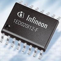
1ED020I12-F Infineon Technologies, 1ED020I12-F Datasheet - Page 8

1ED020I12-F
Manufacturer Part Number
1ED020I12-F
Description
MOSFET & Power Driver ICs SNGL IGBT Driver IC IGBT Driver IC
Manufacturer
Infineon Technologies
Datasheet
1.1ED020I12-F.pdf
(22 pages)
Specifications of 1ED020I12-F
Product
Driver ICs - Various
Rise Time
400 ns
Fall Time
600 ns
Supply Voltage (max)
5.5 V, 20 V, 0 V
Supply Voltage (min)
4.5 V, 13 V, - 12 V
Maximum Power Dissipation
700 mW
Maximum Operating Temperature
+ 105 C
Mounting Style
SMD/SMT
Minimum Operating Temperature
- 40 C
Number Of Drivers
1
Number Of Outputs
1
Package / Case
PG-DSO-16-15
Lead Free Status / RoHS Status
Lead free / RoHS Compliant
Available stocks
Company
Part Number
Manufacturer
Quantity
Price
Company:
Part Number:
1ED020I12-F
Manufacturer:
VISHAY
Quantity:
400 000
Part Number:
1ED020I12-F
Manufacturer:
INFINEON/英飞凌
Quantity:
20 000
Company:
Part Number:
1ED020I12-F2
Manufacturer:
INFINEON
Quantity:
2 190
Part Number:
1ED020I12-F2
Manufacturer:
INFINEON/英飞凌
Quantity:
20 000
Part Number:
1ED020I12-FA
Manufacturer:
INFINEON/英飞凌
Quantity:
20 000
Part Number:
1ED020I12-FT
Manufacturer:
INFINEON/英飞凌
Quantity:
20 000
3.2
GND1
Ground connection of the input side.
IN+ Non-inverting driver input
IN+ control signal for the driver output if IN- is set to low.
(The IGBT is on if IN+ = high and IN- = low)
A minimum pulse width is defined to make the IC robust
against glitches at IN+. An internal Pull-Down-Resistor
ensures IGBT Off-State.
IN- Inverting driver input
IN- control signal for driver output if IN+ is set to high.
(IGBT is on if IN- = low and IN+ = high)
A minimum pulse width is defined to make the IC robust
against glitches at IN-. An internal Pull-Up-Resistor ensures
IGBT Off-State.
/RST (Reset) input
Function 1: Enable/shutdown of the input chip. (The IGBT is
off if /RST = low). A minimum pulse width is defined to
make the IC robust against glitches at IN-.
Function 2: Resets the DESAT-FAULT-state of the chip if
/RST is low for a time T
used to ensure FLT status output.
3
3.1
Pin
Datasheet
10
11
12
13
14
15
16
1
2
3
4
5
6
7
8
9
Symbol
VEE2
DESAT
GND2
NC
VCC2
OUT
CLAMP
VEE2
GND1
IN+
IN-
RDY
FLT
RST
VCC1
GND1
Pin Functionality
Pin Configuration and Functionality
Pin Configuration
Function
Negative power supply output side
Desaturation protection
Signal ground output side
Not connected
Positive power supply output side
Driver output
Miller clamping
Negative power supply output side
Signal ground input side
Non inverted driver input
Inverted driver input
Ready output
Fault output
Reset input
Positive power supply input side
Signal ground input side
RST
. An internal Pull-Up-Resistor is
8
/FLT (Fault output)
Open-drain with internal pull up resistor output to report a
desaturation error of the IGBT (/FLT is low if desaturation
occurs)
RDY (Ready status)
Open-drain with internal pull up resistor output to report the
correct operation of the device. (RDY = high if both chips are
above the UVLO level and the internal chip transmission is
faultless)
VCC1
5V power supply of the input chip
VEE2
Negative power supply pins of the output chip. If no negative
supply voltage is available, both pins have to be connected to
GND2.
DESAT (Desaturation)
Monitoring of the IGBT saturation voltage (V
desaturation caused by short circuits. If OUT is high, V
above a defined value and a certain blanking time has
expired, the desaturation protection is activated and the
IGBT is switched off. The blanking time is adjustable by an
1
2
3
4
5
6
7
8
Figure 4: PG-DSO-16-15
VEE2
DESAT
GND2
NC
VCC2
OUT
CLAMP
VEE2
GND1
GND1
VCC1
/RST
RDY
/FLT
IN+
Version 2.2, 2009-12-03
IN-
EICEDRIVER
16
15
14
13
12
11
10
9
1ED020I12-F
CE
) to detect
CE
TM
is


