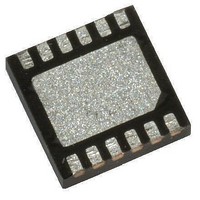
MD1210K6-G Supertex, MD1210K6-G Datasheet - Page 5

MD1210K6-G
Manufacturer Part Number
MD1210K6-G
Description
MOSFET & Power Driver ICs Dual High Speed
Manufacturer
Supertex
Type
High Speed, Dual MOSFET Driverr
Datasheet
1.MD1210K6-G.pdf
(6 pages)
Specifications of MD1210K6-G
Rise Time
6 ns
Fall Time
6 ns
Supply Voltage (min)
4.5 V
Supply Current
6.6 mA
Maximum Operating Temperature
+ 85 C
Mounting Style
SMD/SMT
Minimum Operating Temperature
- 20 C
Number Of Drivers
2
Number Of Outputs
2
Package / Case
QFN-12
Lead Free Status / RoHS Status
Lead free / RoHS Compliant
Application Information
For proper operation of the MD1210, low inductance bypass
capacitors should be used on the various supply pins. The
GND input pin should be connected to the digital ground.
The INA, INB, and OE pins should be connected to their
logic source with a swing of GND to logic level high, which is
1.2V to 5.0V. Good trace practices should be followed cor-
responding to the desired operating speed. The internal cir-
cuitry of the MD1210 is capable of operating up to 100MHz,
with the primary speed limitation being the loading effects
of the load capacitance. Because of this speed and the
high transient currents that result with capacitive loads, the
bypass capacitors should be as close to the chip pins as
possible. The VSS1, VSS2, and VL pins should have low
inductance feed-through connections directly to a ground
plane. The power connections VDD1 and VDD2 should have
a ceramic bypass capacitor to the ground plane with short
leads and decoupling components to prevent resonance in
the power leads. A common capacitor and voltage source
may be used for these two pins, which should always have
the same DC voltage applied. For applications sensitive to
jitter and noise, separate decoupling networks may be used
for VDD1 and VDD2.
Pin Description
Notes:
Pin
10
12
11
1
2
3
4
5
6
7
8
9
1.
2.
Thermal Pad and Pin #5 (VSS1) must be connected externally.
Index Pad and Thermal Pad are connected internally
Name Description
OUTB
OUTA
VDD2 High side gate drive supply voltage.
VDD1 High side analog circuit and level shifter supply voltage. Should be at the same potential as VDD2.
VSS1
VSS2
GND
INB
INA
VH
OE
VL
Logic input. Controls OUTA when OE is high. Input logic high will cause the output to swing to VL. Input
logic low will cause the output to swing to VH.
Supply voltage for N-channel output stage.
Logic input. Controls OUTB when OE is high. Input logic high will cause the output to swing to VL. Input
logic low will cause the output to swing to VH.
Logic input ground reference.
Low side analog circuit and level shifter supply voltage. Should be at the same potential as VSS2.
Low side gate drive supply voltage.
Output driver. Swings from VH to VL. Intended to drive the gate of an external N-channel MOSFET via a
series capacitor. When OE is low, the output is disabled. OUTB will swing to VL turning off the external N-
channel MOSFET.
Supply voltage for P-channel output stage.
Output driver. Swings from VH to VL. Intended to drive the gate of an external P-channel MOSFET via a
series capacitor. When OE is low, the output is disabled. OUTA will swing to VH turning off the external
P-channel MOSFET.
Output-enable logic input. When OE is high, (V
high and low for INA and INB. When OE is low, OUTA is at VH and OUTB is at VL regardless of INA and
INB.
●
1235 Bordeaux Drive, Sunnyvale, CA 94089
5
OE
The VH and VL pins can draw fast transient currents of up to
2.0A, so they should be provided with an appropriate bypass
capacitor located next to the chip pins. A ceramic capacitor
of up to 1.0µF may be appropriate, with a series ferrite bead
to prevent resonance in the power supply lead coming to the
capacitor. Pay particular attention to minimizing trace lengths
and using sufficient trace width to reduce inductance. Sur-
face mount components are highly recommended. Since the
output impedance of this driver is very low, in some cases it
may be desirable to add a small series resistor in series with
the output signal to obtain better waveform integrity at the
load terminals. This will of course reduce the output voltage
slew rate at the terminals of a capacitive load.
Pay particular attention to the parasitic coupling from the
driver output to the input signal terminals. This feedback
may cause oscillations or spurious waveform shapes on the
edges of signal transitions. Since the input operates with sig-
nals down to 1.2V even small coupled voltages may cause
problems. Use of a solid ground plane and good power and
signal layout practices will prevent this problem. Be careful
that the circulating ground return current from a capacitive
load cannot react with common inductance to cause noise
voltages in the input logic circuitry.
+ V
GND
)/2 sets the threshold transition between logic level
●
Tel: 408-222-8888
●
www.supertex.com
MD1210


