MD1210K6-G Supertex, MD1210K6-G Datasheet
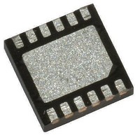
MOSFET & Power Driver ICs Dual High Speed

MD1210K6-G

Manufacturer Part Number
MD1210K6-G
Description
MOSFET & Power Driver ICs Dual High Speed
Manufacturer
Supertex
Type
High Speed, Dual MOSFET Driverr
Datasheet

Specifications of MD1210K6-G

Rise Time
6 ns
Fall Time
6 ns
Supply Voltage (min)
4.5 V
Supply Current
6.6 mA
Maximum Operating Temperature
+ 85 C
Mounting Style
SMD/SMT
Minimum Operating Temperature
- 20 C
Number Of Drivers
2
Number Of Outputs
2
Package / Case
QFN-12
Lead Free Status / RoHS Status
Lead free / RoHS Compliant
Features
Applications
Typical Application Circuit
Logic Inputs
3.3V CMOS
6ns rise and fall time with 1000pF load
2.0A peak output source/sink current
1.2 to 5.0V input CMOS compatible
4.5 to 13V single positive supply voltage
Smartlogic threshold
Low jitter design
Two matched channels
Outputs can swing below ground
Low inductance package
Thermally-enhanced package
Medical ultrasound imaging
Piezoelectric transducer drivers
Nondestructive evaluation
PIN diode driver
CCD clock driver/buffer
High speed level translator
INB
INA
OE
Shifter
Shifter
Shifter
Level
Level
Level
VDD1
GND
High Speed Dual MOSFET Driver
VSS1
1235 Bordeaux Drive, Sunnyvale, CA 94089
VDD2
VSS2
VDD2
VSS2
General Description
The Supertex MD1210 is a high speed, dual MOSFET driver. It is
designed to drive high voltage P and N-channel MOSFET transistors
for medical ultrasound and other applications requiring a high output
current for a capacitive load. The high-speed input stage of the
MD1210 can operate from 1.2 to 5.0V logic interface with an optimum
operating input signal range of 1.8 to 3.3V. An adaptive threshold circuit
is used to set the level translator switch threshold to the average of the
input logic 0 and logic 1 levels. The input logic levels may be ground
referenced, even though the driver is putting out bipolar signals. The
level translator uses a proprietary circuit, which provides DC coupling
together with high-speed operation.
VDD1, VDD2, and VH should be connected to the positive supply
voltage, and VSS1, VSS2, and VL should be connected to 0V or to
Ground. The GND pin is the logic control input signal digital ground.
The output stage is capable of peak currents of up to ±2.0A, depending
on the supply voltages used and load capacitance present.
The OE pin serves a dual purpose. First, its logic H level is used
to compute the threshold voltage level for the channel input level
translators. Secondly, when OE is low, the outputs are disabled, with
the A output high and the B output low. This assists in properly pre-
charging the AC coupling capacitors that may be used in series in the
gate drive circuit of an external PMOS and NMOS transistor pair.
VL
VH
VL
VH
OUTA
OUTB
Supertex
MD1210
+12V
0.47µF
10nF
10nF
Tel: 408-222-8888
TC6320TG
Supertex
www.supertex.com
+100V
-100V
1.0µF
1.0µF
MD1210
To Piezoelectric
Transducer

Related parts for MD1210K6-G

MD1210K6-G Summary of contents

Page 1

... Shifter GND VSS1 General Description The Supertex MD1210 is a high speed, dual MOSFET driver designed to drive high voltage P and N-channel MOSFET transistors for medical ultrasound and other applications requiring a high output current for a capacitive load. The high-speed input stage of the MD1210 can operate from 1.2 to 5.0V logic interface with an optimum operating input signal range of 1 ...

Page 2

... Ordering Information Package Option 12-Lead QFN Device 4.00x4.00mm body 1.00mm height (max) 0.80mm pitch MD1210 MD1210K6-G -G indicates package is RoHS compliant (‘Green’) Absolute Maximum Ratings Parameter supply voltage DD1 DD2 supply voltage SS1 SS2 L Logic input levels Maximum junction temperature Storage temperature ...

Page 3

... V = 3.3V 25°C) SS1 SS2 OE A Max Units Conditions Logic input edge speed require ment - 1000pF, LOAD see timing diagram - ns Input signal rise/fall time of 2ns - For each channel - Device to device delay match Output OUTA ● Tel: 408-222-8888 ● www.supertex.com MD1210 OUTB ...

Page 4

... SUB GND VSS1 VSS2 ● 1235 Bordeaux Drive, Sunnyvale, CA 94089 4 VDD1 VDD2 VH MD1210 OE INA INB GND VSS1 VSS2 1.5 1.0 0.6V 0.5 0 1.0 2.0 4.0 3.0 5.0 V (volts OUTA VL VH OUTB VL ● Tel: 408-222-8888 ● www.supertex.com MD1210 OUTA OUTB ...

Page 5

... V OE GND ● 1235 Bordeaux Drive, Sunnyvale, CA 94089 5 )/2 sets the threshold transition between logic level ● Tel: 408-222-8888 ● www.supertex.com MD1210 ...

Page 6

... Supertex inc. does not recommend the use of its products in life support applications, and will not knowingly sell them for use in such applications unless it receives an adequate “product liability indemnification insurance agreement.” Supertex inc. does not assume responsibility for use of devices described, and limits its liability to the replacement of the devices determined defective due to workmanship ...

Related keywords