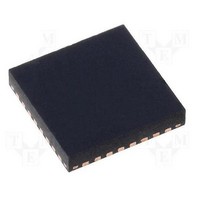
MAX5978ETJ+ Maxim Integrated Products, MAX5978ETJ+ Datasheet - Page 28

MAX5978ETJ+
Manufacturer Part Number
MAX5978ETJ+
Description
Hot Swap & Power Distribution 0-16V HOTSWAP CONTLR W/10BIT CUR VOLT MON
Manufacturer
Maxim Integrated Products
Datasheet
1.MAX5978ETJ.pdf
(38 pages)
Specifications of MAX5978ETJ+
Product
Controllers & Switches
Supply Voltage (max)
16 V
Supply Voltage (min)
0 V
Power Dissipation
2759 mW
Operating Temperature Range
- 40 C to + 85 C
Mounting Style
SMD/SMT
Supply Current
2.5 mA
Package / Case
TQFN-32
Lead Free Status / RoHS Status
Lead free / RoHS Compliant
0 to 16V, Hot-Swap Controller with 10-Bit
Current, Voltage Monitor, and 4 LED Drivers
The five digital comparators (undervoltage/overvoltage
warning and critical, overcurrent warning) all have a
user-selectable deglitching feature that requires two
consecutive positive compares before the device takes
action as determined by the particular compare and the
setting of the PROT input.
The deglitching functions are enabled or disabled by
registers dgl_i, dgl_uv, and dgl_ov (Tables 37, 38, and
39). Writing a 1 to the appropriate bit location in these
registers enables the deglitch function for the corre-
sponding digital comparator.
The device features two 10-bit “circular buffers” (in vola-
tile memory) that contain a history of the 50 most-recent
voltage and current digital-conversion results. These cir-
cular buffers can be read back through the I
Table 37. OI Warning Comparators Deglitch Enable Register Format
Table 38. UV Warning and Critical Comparators Deglitch Enable Register Format
Table 39. OV Warning and Critical Comparators Deglitch Enable Register Format
28
Description:
Register Title:
Register Address:
Description:
Register Title:
Register Address:
Description:
Register Title:
Register Address:
Bit 7
Bit 7
Bit 7
—
—
—
R
R
R
Deglitching of Digital Comparators
Bit 6
Bit 6
Bit 6
—
—
—
R
R
R
Deglitch enable register for undervoltage warning and critical digital comparators
dgl_uv
0x3D
Deglitch enable register for overvoltage warning and critical digital comparators
dgl_ov
0x3E
Deglitch enable register for overcurrent warning digital comparators
dgl_i
0x3C
Bit 5
Bit 5
Bit 5
—
—
—
R
R
R
Circular Buffer
2
Bit 4
Bit 4
Bit 4
C interface.
—
—
R
—
R
R
Unused
Unused
Bit 3
R/W
Bit 3
R/W
Bit 3
—
R
The recording of new data to the buffer for a given signal
is stopped under any of the following conditions:
• The hot-swap channel is shut down because of a fault
• A read of the circular buffer base address is per-
• The hot-swap channel is turned off by a combination
The buffers allow the user to recall the voltage and cur-
rent waveforms for analysis and troubleshooting. The
buffer contents are accessed through the I
at two fixed addresses in the device register address
space (see Table 40).
Each buffer can also be stopped under user control by
register cbuf_chx_store (see Table 41).
condition.
formed through the I
of the EN1, EN2, or ON signals.
Unused
Unused
R/W
Bit 2
Bit 2
Bit 2
R/W
—
R
dgl_uv2
dgl_ov2
Unused
Bit 1
R/W
Bit 1
Bit 1
R/W
R/W
2
C interface.
dgl_uv1
dgl_ov1
Bit 0
R/W
dgl_i
R/W
Bit 0
R/W
Bit 0
2
RESET
VALUE
C interface
RESET
VALUE
RESET
VALUE
0x00
0x00
0x00
—
—
—


