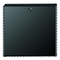
PIC18F6585-I/L Microchip Technology, PIC18F6585-I/L Datasheet - Page 29

PIC18F6585-I/L
Manufacturer Part Number
PIC18F6585-I/L
Description
Microcontrollers (MCU) 48KB 3328 RAM 52 I/O
Manufacturer
Microchip Technology
Datasheet
1.PCM18XK1.pdf
(496 pages)
Specifications of PIC18F6585-I/L
Processor Series
PIC18F
Core
PIC
Data Bus Width
8 bit
Data Ram Size
3.25 KB
Interface Type
I2C/SPI/AUSART/CAN
Maximum Clock Frequency
40 MHz
Number Of Programmable I/os
53
Number Of Timers
5
Maximum Operating Temperature
+ 85 C
Mounting Style
SMD/SMT
3rd Party Development Tools
52715-96, 52716-328, 52717-734, 52712-325, EWPIC18
Development Tools By Supplier
PG164130, DV164035, DV244005, DV164005, PG164120, ICE2000, ICE4000, DV164136, DM183032
Minimum Operating Temperature
- 40 C
On-chip Adc
12-ch x 10-bit
Program Memory Type
Flash
Program Memory Size
48 KB
Package / Case
PLCC-68
Lead Free Status / RoHS Status
Lead free / RoHS Compliant
- Current page: 29 of 496
- Download datasheet (9Mb)
2.6.1
The system clock source switching is performed under
software control. The System Clock Switch bits,
SCS1:SCS0 (OSCCON<1:0>), control the clock switch-
ing. When the SCS0 bit is ‘0’, the system clock source
comes from the main oscillator that is selected by the
FOSC configuration bits in configuration register,
CONFIG1H. When the SCS0 bit is set, the system clock
source will come from the Timer1 oscillator. The SCS0
bit is cleared on all forms of Reset.
When FOSC bits are programmed for software PLL
mode, the SCS1 bit can be used to select between pri-
mary oscillator/clock and PLL output. The SCS1 bit will
only have an effect on the system clock if the PLL is
REGISTER 2-1:
2004 Microchip Technology Inc.
SYSTEM CLOCK SWITCH BIT
bit 7-4 Unimplemented: Read as ‘0’
bit 3
bit 2
bit 1
bit 0
OSCCON REGISTER
bit 7
LOCK: Phase Lock Loop Lock Status bit
1 = Phase Lock Loop output is stable as system clock
0 = Phase Lock Loop output is not stable and output cannot be used as system clock
PLLEN
1 = Enable Phase Lock Loop output as system clock
0 = Disable Phase Lock Loop
SCS1: System Clock Switch bit 1
When PLLEN and LOCK bits are set:
1 = Use PLL output
0 = Use primary oscillator/clock input pin
When PLLEN or LOCK bit is cleared:
Bit is forced clear.
SCS0
When OSCSEN configuration bit = 0 and T1OSCEN bit = 1:
1 = Switch to Timer1 oscillator/clock pin
0 = Use primary oscillator/clock input pin
When OSCSEN and T1OSCEN are in other states:
Bit is forced clear.
Legend:
R = Readable bit
- n = Value at POR
Note 1: PLLEN bit is ignored when configured for ECIO+PLL and HS+PLL. This bit is used
U-0
—
(2)
(1)
2: The setting of SCS0 = 1 supersedes SCS1 = 1.
: System Clock Switch bit 0
: Phase Lock Loop Enable bit
in ECIO+SPLL and HS+SPLL modes only.
U-0
—
PIC18F6585/8585/6680/8680
W = Writable bit
‘1’ = Bit is set
U-0
—
enabled (PLLEN = 1) and locked (LOCK = 1), else it will
be forced clear. When programmed with Configuration
Controlled PLL mode, the SCS1 bit will be forced clear.
U-0
—
Note:
U = Unimplemented bit, read as ‘0’
‘0’ = Bit is cleared
R/W-0
The Timer1 oscillator must be enabled
and operating to switch the system clock
source. The Timer1 oscillator is enabled
by setting the T1OSCEN bit in the Timer1
Control register (T1CON). If the Timer1
oscillator is not enabled, then any write to
the SCS0 bit will be ignored (SCS0 bit
forced cleared) and the main oscillator will
continue to be the system clock source.
LOCK
PLLEN
R/W-0
x = Bit is unknown
R/W-0
SCS1
DS30491C-page 27
R/W-0
SCS0
bit 0
Related parts for PIC18F6585-I/L
Image
Part Number
Description
Manufacturer
Datasheet
Request
R

Part Number:
Description:
20-Pin USB Flash Microcontrollers
Manufacturer:
MICROCHIP [Microchip Technology]
Datasheet:

Part Number:
Description:
PIC18F With 128-segment LCD Driver And 12-bit ADC, 8KB Flash, 768B RAM, CCP, MSS
Manufacturer:
Microchip Technology
Datasheet:

Part Number:
Description:
PIC18F With 128-segment LCD Driver And 12-bit ADC, 16KB Flash, 768B RAM, CCP, MS
Manufacturer:
Microchip Technology
Datasheet:

Part Number:
Description:
PIC18F With 192-segment LCD Driver And 12-bit ADC, 8KB Flash, 768B RAM, CCP, MSS
Manufacturer:
Microchip Technology
Datasheet:

Part Number:
Description:
PIC18F With 192-segment LCD Driver And 12-bit ADC, 16KB Flash, 768B RAM, CCP, MS
Manufacturer:
Microchip Technology
Datasheet:

Part Number:
Description:
Microcontrollers (MCU) 64KB 3328 RAM 52 I/O
Manufacturer:
Microchip Technology
Datasheet:

Part Number:
Description:
32kB Flash, 2kB RAM, 1kB EE, NanoWatt XLP, LCD 64 QFN 9x9x0.9mm T/R
Manufacturer:
Microchip Technology
Datasheet:

Part Number:
Description:
32kB Flash, 2kB RAM, 1kB EE, NanoWatt XLP, LCD 64 TQFP 10x10x1mm T/R
Manufacturer:
Microchip Technology
Datasheet:

Part Number:
Description:
128kB Flash, 4kB RAM, 1kB EE, 16MIPS, NanoWatt XLP, LCD, 5V 80 TQFP 12x12x1mm T/
Manufacturer:
Microchip Technology
Datasheet:

Part Number:
Description:
32kB Flash, 2kB RAM, 1kB EE, NanoWatt XLP, LCD 64 QFN 9x9x0.9mm TUBE
Manufacturer:
Microchip Technology
Datasheet:

Part Number:
Description:
32kB Flash, 2kB RAM, 1kB EE, NanoWatt XLP, LCD 64 TQFP 10x10x1mm TRAY
Manufacturer:
Microchip Technology

Part Number:
Description:
128kB Flash, 4kB RAM, 1kB EE, 16MIPS, NanoWatt XLP, LCD, 5V 80 TQFP 12x12x1mm TR
Manufacturer:
Microchip Technology

Part Number:
Description:
Manufacturer:
Microchip Technology Inc.
Datasheet:


