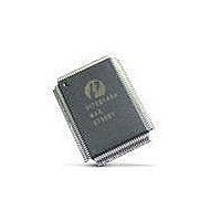
PI7C21P100BNHE Pericom Semiconductor, PI7C21P100BNHE Datasheet - Page 18

PI7C21P100BNHE
Manufacturer Part Number
PI7C21P100BNHE
Description
Peripheral Drivers & Components (PCIs) PCI-X to PCI-XBridge 2 Port
Manufacturer
Pericom Semiconductor
Datasheet
1.PI7C21P100BNHE.pdf
(79 pages)
Specifications of PI7C21P100BNHE
Maximum Operating Temperature
+ 70 C
Minimum Operating Temperature
0 C
Mounting Style
SMD/SMT
Operating Supply Voltage
3 V to 3.6 V
Package / Case
CSBGA-304
Lead Free Status / RoHS Status
Lead free / RoHS Compliant
Available stocks
Company
Part Number
Manufacturer
Quantity
Price
Company:
Part Number:
PI7C21P100BNHE
Manufacturer:
Pericom
Quantity:
135
Company:
Part Number:
PI7C21P100BNHE
Manufacturer:
PI
Quantity:
1 831
3.2.8
3.2.9
TEST SIGNALS
POWER AND GROUND SIGNALS
Name
TRST#
Name
T_DI1
T_DI2
T_MODECTL
T_RI
XCLK_OUT
T_RI
TEST_CE0
Name
P_VDDA
P_VSSA
S_VDDA
Pin #
C23
Pin #
Y21
AA4
C1
W22
D3
W22
Y23
Pin #
A21
D16
AB21
Page 18 of 79
Type
Type
Type
IU
IU
IU
ID
P
P
P
I
I
I
I
Description
Test Reset. Active LOW signal to reset the Test Access
Port (TAP) controller into an initialized state.
Description
PLL Bypass Control for PCI-X Mode. The strapped
value of this pin (at P_RST# deassertion) controls
whether the internal PLL’s are bypassed in PCI-X mode.
HIGH: PLL’s are used in PCI-X mode
LOW: PLL’s are bypassed in PCI-X mode
Shorten Initialization Period. Controls the period for
the following signals during initialization.
LOW: Shorten periods
HIGH: Normal initialization
PLL Test Control. Controls along with the internal
PLL testing.
* P_PLL enabled, S_PLL disabled
**P_PLL disabled, S_PLL enabled
PLL Bypass Control for PCI Mode. The strapped
value of this pin (at T_RI) controls whether the internal
PLL’s are bypassed in PCI mode.
1: PLL’s are bypassed in PCI mode
0 and T_MODECTL=0: PLL’s are used in PCI mode
Scan Chain Enable. Used as SCAN_EN with
SCAN_TM being controlled by JTAG instruction.
S_REQ[6:2] are used as the data inputs of 5 scan chains
S_GNT[6:2] are used as the data ouputs of 5 scan chains
Description
2.5V Power: Power supply to the PLL for the primary
clock domain.
2.5V Power: Ground for the PLL for the primary clock
domain.
2.5V Power: Power supply to the PLL for the secondary
clock domain.
T_RI
T
T
T
T
T
T
T
T
PIRSTDLY
XCAP
SIRSTDLY
SRSTDLY
PIRSTDLY
XCAP
SIRSTDLY
SRSTDLY
H
H
L
2-PORT PCI-X TO PCI-X BRIDGE
– See Table 7-2
– 6 Primary Clocks
– See Table 7-2
– See Table 7-2
– See Table 7-2
T_MODECTL
– 11 Secondary Clocks + 7 Primary Clocks
- 5 Primary Clocks
- 40 Secondary Clocks
November 2005 – Revision 1.02
H
H
L
XCLK_OUT
S_CLK**
P_CLK*
Z
PI7C21P100B


