SSM3K105TU(TE85L) Toshiba, SSM3K105TU(TE85L) Datasheet
SSM3K105TU(TE85L)
Manufacturer Part Number
SSM3K105TU(TE85L)
Description
MOSFET Small Signal Vds=30V Id=2.1A 3Pin
Manufacturer
Toshiba
Datasheet
1.SSM3K105TUTE85L.pdf
(5 pages)
Specifications of SSM3K105TU(TE85L)
Configuration
Single
Transistor Polarity
N-Channel
Resistance Drain-source Rds (on)
0.15 Ohms
Forward Transconductance Gfs (max / Min)
2 S / 1 S
Drain-source Breakdown Voltage
30 V
Continuous Drain Current
2.1 A
Power Dissipation
800 mW
Mounting Style
SMD/SMT
Package / Case
UFM
Lead Free Status / RoHS Status
Lead free / RoHS Compliant
Available stocks
Company
Part Number
Manufacturer
Quantity
Price

Part Number:
SSM3K105TU(TE85L)
Manufacturer:
TOSHIBA/东芝
Quantity:
20 000


High Speed Switching Applications
•
•
•
Maximum Ratings
Electrical Characteristics
Note1: Mounted on ceramic board.
Note2: Mounted on FR4 board.
Note3: Pulse test
4V drive
Low on-resistance:
Lead(Pb)-free
Drain-Source voltage
Gate-Source voltage
Drain current
Drain power dissipation
Channel temperature
Storage temperature range
Drain-Source breakdown voltage
Drain cut-off current
Gate leakage current
Gate threshold voltage
Forward transfer admittance
Drain-Source on-resistance
Input capacitance
Output capacitance
Reverse transfer capacitance
Switching time
Drain-Source forward voltage
(25.4 mm × 25.4 mm × 0.8 mm, Cu Pad: 645 mm
(25.4 mm × 25.4 mm × 1.6 mm, Cu Pad: 645 mm
Characteristic
Characteristic
Turn-on time
Turn-off time
TOSHIBA Field Effect Transistor Silicon N Channel MOS Type
(Ta = 25°C)
DC
Pulse
R
R
R
on
on
on
= 480mΩ (max) (@V
= 200mΩ (max) (@V
= 110mΩ (max) (@V
(Ta = 25°C)
SSM3K105TU
V
R
P
P
Symbol
(BR) DSS
Symbol
⏐Y
DS (ON)
V
D (Note1)
D (Note2)
I
I
C
V
C
C
GSS
DSS
V
V
t
t
T
DSF
T
I
oss
on
off
GSS
rss
I
DP
iss
stg
th
fs
DS
D
ch
⏐
I
V
V
V
V
I
I
I
V
V
V
V
V
I
D
D
D
D
D
GS
GS
GS
DS
GS
DS
DS
DS
DS
DS
DD
GS
= 1 mA, V
= 0.75 A, V
= 0.75 A, V
= 0.75 A, V
= −2.1A, V
= 30 V, V
= 5 V, I
= 5 V, I
= 15 V, V
= 15 V, V
= 15 V, V
−55~150
= ±16V, V
= 15 V, I
= 0~4 V, R
= 10V)
= 3.3V)
= 4V)
Rating
± 20
800
500
150
2.1
4.2
30
1
2
2
D
D
)
)
Test Conditions
GS
GS
D
GS
GS
GS
GS
= 0.1 mA
= 0.75 A
GS
GS
GS
DS
= 0.75 A,
G
= 0
= 0 V
= 10 V
= 4 V
= 3.3 V
= 0
= 0, f = 1 MHz
= 0, f = 1 MHz
= 0, f = 1 MHz
= 10 Ω
= 0
Unit
mW
°C
°C
V
V
A
(Note3)
(Note3)
(Note3)
(Note3)
(Note3)
Weight: 6.6 mg (typ.)
JEDEC
JEITA
TOSHIBA
UFM
Min
1.1
1.0
30
⎯
⎯
⎯
⎯
⎯
⎯
⎯
⎯
⎯
⎯
⎯
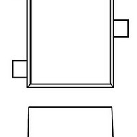
1 :Gate
2 :Source
3 :Drain
−0.95
SSM3K105TU
1
2
Typ.
150
210
102
2.0
85
57
22
46
65
⎯
⎯
⎯
⎯
2.1±0.1
1.7±0.1
2-2U1A
2005-04-12
―
―
Max
−
110
200
480
1.8
±1
⎯
⎯
⎯
⎯
⎯
⎯
⎯
1.3
1
Unit: mm
3
Unit
mΩ
µA
µA
pF
pF
pF
ns
V
V
S
V
Related parts for SSM3K105TU(TE85L)
Image
Part Number
Description
Manufacturer
Datasheet
Request
R

Part Number:
Description:
Silicon N Channel Mos Type High Speed Switching Applications
Manufacturer:
TOSHIBA Semiconductor CORPORATION
Datasheet:
Part Number:
Description:
Toshiba Semiconductor [TOSHIBA IGBT Module Silicon N Channel IGBT]
Manufacturer:
TOSHIBA Semiconductor CORPORATION
Datasheet:
Part Number:
Description:
TOSHIBA GTR MODULE SILICON NPN TRIPLE DIFFUSED TYPE
Manufacturer:
TOSHIBA Semiconductor CORPORATION
Datasheet:
Part Number:
Description:
TOSHIBA GTR Module Silicon N Channel IGBT
Manufacturer:
TOSHIBA Semiconductor CORPORATION
Datasheet:
Part Number:
Description:
TOSHIBA Intelligent Power Module Silicon N Channel IGBT
Manufacturer:
TOSHIBA Semiconductor CORPORATION
Datasheet:
Part Number:
Description:
TOSHIBA INTELLIGENT POWER MODULE SILICON N CHANNEL LGBT
Manufacturer:
TOSHIBA Semiconductor CORPORATION
Datasheet:
Part Number:
Description:
TOSHIBA IGBT Module Silicon N Channel IGBT
Manufacturer:
TOSHIBA Semiconductor CORPORATION
Datasheet:
Part Number:
Description:
TOSHIBA GTR MODULE SILICON N−CHANNEL IGBT
Manufacturer:
TOSHIBA Semiconductor CORPORATION
Datasheet:
Part Number:
Description:
TOSHIBA Intelligent Power Module Silicon N Channel IGBT
Manufacturer:
TOSHIBA Semiconductor CORPORATION
Datasheet:
Part Number:
Description:
TOSHIBA GTR Module Silicon N Channel IGBT
Manufacturer:
TOSHIBA Semiconductor CORPORATION
Datasheet:
Part Number:
Description:
TOSHIBA INTELLIGENT POWER MODULE
Manufacturer:
TOSHIBA Semiconductor CORPORATION
Datasheet:
Part Number:
Description:
TOSHIBA Intelligent Power Module Silicon N Channel IGBT
Manufacturer:
TOSHIBA Semiconductor CORPORATION
Datasheet:
Part Number:
Description:
TOSHIBA Intelligent Power Module Silicon N Channel IGBT
Manufacturer:
TOSHIBA Semiconductor CORPORATION
Datasheet:
Part Number:
Description:
TOSHIBA IGBT Module Silicon N Channel IGBT
Manufacturer:
TOSHIBA Semiconductor CORPORATION
Datasheet:
Part Number:
Description:
TOSHIBA Intelligent Power Module Silicon N Channel IGBT
Manufacturer:
TOSHIBA Semiconductor CORPORATION
Datasheet:
SSM3K105TU(TE85L) Summary of contents
Page 1
... TOSHIBA Field Effect Transistor Silicon N Channel MOS Type SSM3K105TU High Speed Switching Applications • 4V drive • Low on-resistance 480mΩ (max) (@ 200mΩ (max) (@ 110mΩ (max) (@V on • Lead(Pb)-free Maximum Ratings (Ta = 25°C) Characteristic Drain-Source voltage Gate-Source voltage DC Drain current ...
Page 2
Switching Time Test Circuit (a) Test Circuit µ Ω D.U. < < Common Source ...
Page 3
SSM3K105TU 3 2005-04-12 ...
Page 4
1000 a: mounted on FR4 board (25.4mm×25.4mm×1.6mm) Cu Pad :25.4mm×25.4mm b 800 b:mounted on ceramic board (25.4mm×25.4mm×0.8mm) Cu Pad :25.4mm×25.4mm 600 a 400 200 100 120 140 160 Ambient temperature Ta(°C) ...
Page 5
SSM3K105TU 5 2005-04-12 ...