A000046 Arduino, A000046 Datasheet - Page 19
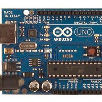
A000046
Manufacturer Part Number
A000046
Description
MCU, MPU & DSP Development Tools Uno
Manufacturer
Arduino
Series
-r
Type
MCUr
Specifications of A000046
Processor To Be Evaluated
ATmega328
Interface Type
USB, I2C, SPI
Dimensions
2.7 in x 2.1 in
Operating Supply Voltage
5 V
Contents
Board
Lead Free Status / RoHS Status
Lead free / RoHS Compliant
For Use With/related Products
ATmega328


7.3.1
7.4
7.4.1
8161D–AVR–10/09
EEPROM Data Memory
Data Memory Access Times
EEPROM Read/Write Access
This section describes the general access timing concepts for internal memory access. The
internal data SRAM access is performed in two clk
Figure 7-4.
The ATmega48PA/88PA/168PA/328P contains 256/512/512/1K bytes of data EEPROM mem-
ory. It is organized as a separate data space, in which single bytes can be read and written. The
EEPROM has an endurance of at least 100,000 write/erase cycles. The access between the
EEPROM and the CPU is described in the following, specifying the EEPROM Address Regis-
ters, the EEPROM Data Register, and the EEPROM Control Register.
”Memory Programming” on page 294
in SPI or Parallel Programming mode.
The EEPROM Access Registers are accessible in the I/O space.
The write access time for the EEPROM is given in
lets the user software detect when the next byte can be written. If the user code contains instruc-
tions that write the EEPROM, some precautions must be taken. In heavily filtered power
supplies, V
period of time to run at a voltage lower than specified as minimum for the clock frequency used.
See
situations.
In order to prevent unintentional EEPROM writes, a specific write procedure must be followed.
Refer to the description of the EEPROM Control Register for details on this.
When the EEPROM is read, the CPU is halted for four clock cycles before the next instruction is
executed. When the EEPROM is written, the CPU is halted for two clock cycles before the next
instruction is executed.
”Preventing EEPROM Corruption” on page 20
CC
Address
clk
is likely to rise or fall slowly on power-up/down. This causes the device for some
On-chip Data SRAM Access Cycles
Data
Data
WR
CPU
RD
Compute Address
T1
Memory Access Instruction
ATmega48PA/88PA/168PA/328P
contains a detailed description on EEPROM Programming
Address valid
CPU
for details on how to avoid problems in these
T2
Table
cycles as described in
7-2. A self-timing function, however,
Next Instruction
T3
Figure
7-4.
19
Related parts for A000046
Image
Part Number
Description
Manufacturer
Datasheet
Request
R

Part Number:
Description:
Daughter Cards & OEM Boards ARDUINO UNO PROTO PCB REV 3
Manufacturer:
Arduino
Part Number:
Description:
Daughter Cards & OEM Boards ARDUINO SHIELD PROTO KIT REV 3
Manufacturer:
Arduino
Part Number:
Description:
Daughter Cards & OEM Boards ARDUINO MEGA PROTO KIT REV 3
Manufacturer:
Arduino
Part Number:
Description:
Daughter Cards & OEM Boards ARDUINO MEGA PROTO PCB REV 3
Manufacturer:
Arduino
Part Number:
Description:
Development Boards & Kits - AVR ARDUINO STARTER KIT W/ UNO REV3
Manufacturer:
Arduino
Part Number:
Description:
RF Development Tools ARDUINO SHIELD WIRELESS PROTO
Manufacturer:
Arduino
Datasheet:
Part Number:
Description:
RF Development Tools ARDUINO SHIELD WIRELESS WITH SD
Manufacturer:
Arduino
Datasheet:

Part Number:
Description:
Development Software Getting started w/Arduino
Manufacturer:
Arduino

Part Number:
Description:
Ethernet Modules & Development Tools Ethernet Shield for Arduino
Manufacturer:
Arduino

Part Number:
Description:
MCU, MPU & DSP Development Tools LilyPad Arduino Main Board
Manufacturer:
Arduino

Part Number:
Description:
ARDUINO NANO Board
Manufacturer:
Arduino
Datasheet:
Part Number:
Description:
Ethernet Modules & Development Tools ETHERNET SHEILD PoE FOR ARDUINO
Manufacturer:
Arduino
Datasheet:

Part Number:
Description:
ATMEGA328 MCU IC W/ Arduino UNO Bootloader
Manufacturer:
Arduino
Datasheet:
Part Number:
Description:
Memory Cards MICRO SD CARD 1GB WITH SD ADAPTER
Manufacturer:
Arduino