RDK-242 Power Integrations, RDK-242 Datasheet - Page 10
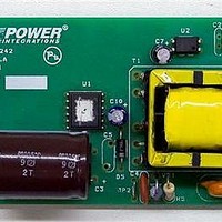
RDK-242
Manufacturer Part Number
RDK-242
Description
Power Management Modules & Development Tools TOPSwitch-JX REF. DESIGN KIT
Manufacturer
Power Integrations
Type
MOSFET & Power Driverr
Datasheet
1.RDK-242.pdf
(59 pages)
Specifications of RDK-242
Input Voltage
85 VAC to 264 VAC
Output Voltage
12 V
Maximum Operating Temperature
+ 40 C
Minimum Operating Temperature
0 C
Operating Supply Voltage
85 VAC to 264 VAC
Product
Power Management Modules


4.1.5 Feedback Configuration
• A high CTR optocoupler was used to reduce secondary bias currents and no-load input
• Low voltage, low current voltage reference IC used on secondary side to reduce
• Bias winding voltage tuned to ~9 V at no-load, high line to reduce no-load input power
Typically the feedback current into the CONTROL pin at high line is ~3 mA. This current
is both sourced from the bias winding (voltage across C10) and directly from the output.
Both of these represent a load on the output of the power supply.
To minimize the dissipation from the bias winding under no-load conditions the number of
bias winding turns and value of C7 was adjusted to give a minimum voltage across C7 of
~9 V. This was the minimum achievable to keep the optocoupler biased and the output in
regulation.
To minimize the dissipation of the secondary side feedback circuit a high CTR (CTR of
300 – 600%) optocoupler type was used. This reduces the secondary side opto-led
current from ~3 mA to <~1 mA and therefore the effective load on the output. A standard
2.5 V TL431 voltage reference was replaced with the 1.24 V LMV431 to reduce the
supply current requirement of this component from 1 mA to 100 A
4.1.6 Output Rectifier Choice
• Use of high V
The higher BV
rating of typical power MOSFETs) allowed a higher transformer primary to secondary
turns ratio (reflected output voltage or V
and allowed the use of cheaper and more efficient 60 V (vs 80 V or 100 V) Schottky
diodes. The efficiency improvement occurs due the lower forward voltage drop of the
lower voltage diodes. Two parallel connected axial 5 A, 60 V Schottky rectifier diodes
were selected for both low cost and high efficiency. This allowed PCB heatsinking of the
diode for low cost while maintaining efficiency compared to a single higher current TO-
220 packaged diode mounted on a heatsink. For this configuration the recommendation
is that each diode is rated at twice the output current and that the diodes share a
common cathode PCB area for heatsinking so that their temperatures track. In practice
the diodes current share quite effectively as can be demonstrated by monitoring their
individual temperatures.
power
secondary side feedback current and no-load input power.
cost
Power Integrations, Inc.
Tel: +1 408 414 9200 Fax: +1 408 414 9201
www.powerint.com
DSS
OR
enabled the use of a 60 V Schottky diode for high efficiency and lower
rating of the TOPSwitch-JX of 725 V (compared to 600 V or 650 V
OR
). This reduced the output diode voltage stress
Page 10 of 59
Related parts for RDK-242
Image
Part Number
Description
Manufacturer
Datasheet
Request
R

Part Number:
Description:
KIT REF DESIGN TOP HX FOR TOP258
Manufacturer:
Power Integrations
Datasheet:

Part Number:
Description:
KIT REF DESIGN LINKSWITCH 2
Manufacturer:
Power Integrations
Datasheet:

Part Number:
Description:
KIT REF DESIGN 1.2W PS TN FAMILY
Manufacturer:
Power Integrations
Datasheet:

Part Number:
Description:
KIT REF DESIGN 36-72W MOTOR DRVR
Manufacturer:
Power Integrations
Datasheet:

Part Number:
Description:
KIT REF DESIGN FOR LNK457D
Manufacturer:
Power Integrations
Datasheet:

Part Number:
Description:
REFERENCE DESIGN LINKSWITCH-PH
Manufacturer:
Power Integrations
Datasheet:

Part Number:
Description:
Specifications: Manufacturer: Power Integrations ; Output Voltage: 380 VDC ; Input / Supply Voltage (Max): 264 VAC ; Input / Supply Voltage (Min): 90 VAC ; Mounting Style: Through Hole ; Output Current: 0.913 A ; Output Power: 347 W
Manufacturer:
Power Integrations, Inc.
Part Number:
Description:
Power Management IC Development Tools REF DESIGN RDR-292 PFF LED STREET LIGHT
Manufacturer:
Power Integrations

Part Number:
Description:
KIT REF DESIGN FOR LNK403EG
Manufacturer:
Power Integrations
Datasheet:

Part Number:
Description:
KIT REF DESIGN FOR LNK406EG
Manufacturer:
Power Integrations
Datasheet:

Part Number:
Description:
KIT REF DESIGN DG CAPZERO
Manufacturer:
Power Integrations
Datasheet:

Part Number:
Description:
KIT REF DESIGN LINKSWITCH-CV
Manufacturer:
Power Integrations
Datasheet:

Part Number:
Description:
KIT REF DESIGN PFS762HG
Manufacturer:
Power Integrations
Datasheet:
Part Number:
Description:
Specifications: Family: Eval Boards - DC/DC & AC/DC (Off-Line) SMPS ; Series: HiperLCS™ ; Main Purpose: DC/DC, Step Down ; Outputs and Type: 1, Isolated ; Power - Output: 150W ; Voltage - Output: 24V ; Current - Output: 6.25A ; Voltage - Input:
Manufacturer:
Power Integrations, Inc.
Datasheet:

Part Number:
Description:
KIT REFERENCE DESIGN W/TN376PN
Manufacturer:
Power Integrations
Datasheet: