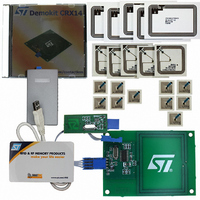
DEMOKITCRX14 STMicroelectronics, DEMOKITCRX14 Datasheet - Page 9
DEMOKITCRX14
Manufacturer Part Number
DEMOKITCRX14
Description
RFID EVALUATION KIT ISO14443-B
Manufacturer
STMicroelectronics
Type
Development kitr
Specifications of DEMOKITCRX14
Contents
CD-ROM, CRX14 Board, USB Transceiver, Samples and Documentation
Processor To Be Evaluated
CRX14
Interface Type
I2C
Operating Supply Voltage
5 V
For Use With/related Products
CRX14
Lead Free Status / RoHS Status
Contains lead / RoHS non-compliant
Other names
497-3704
Available stocks
Company
Part Number
Manufacturer
Quantity
Price
Company:

Part Number:
DEMOKITCRX14
Manufacturer:
HITACHI
Quantity:
340


CRX14
2
2.1
2.2
2.3
2.4
2.5
Signal description
See
connected to this device.
Oscillator (OSC1, OSC2)
The OSC1 and OSC2 pins are internally connected to the on-chip oscillator circuit. The
OSC1 pin is the input pin, the OSC2 is the output pin. For correct operation of the CRX14, it
is required to connect a 13.56MHz quartz crystal across OSC1 and OSC2. If an external
clock is used, it must be connected to OSC1 and OSC2 must be left open.
Antenna output driver (RF
The Antenna Output Driver pin, RF
antenna. Care must be taken as it will not withstand a short-circuit.
RF
application schematic
and GND.
Antenna input filter (RF
The antenna input filter of the CRX14, RF
through an adapter circuit, as shown in
The input filter demodulates the signal generated on the antenna by the load variation of the
PICC. The resulting signal is then decoded by the 847kHz BPSK decoder.
Transmitter reference voltage (V
The Transmitter Reference Voltage input, V
output driver for ASK modulation.
The Transmitter Reference Voltage input should be connected to an external capacitor, as
shown in
Serial clock (SCL)
The SCL input pin is used to strobe all I²C data in and out of the CRX14. In applications
where this line is used by slave devices to synchronize the bus to a slower clock, the master
must have an open drain output, and a pull-up resistor must be connected from the Serial
Clock (SCL) to V
calculated).
In most applications, though, this method of synchronization is not employed, and so the
pull-up resistor is not necessary, provided that the master has a push-pull (rather than open
drain) output.
OUT
Figure 1: Logic
has to be connected to the antenna circuitry as shown in
Figure
4.
CC
.
diagram, and
(Figure 5
The LRC antenna circuitry must be connected across the RF
indicates how the value of the pull-up resistor can be
Doc ID 8880 Rev 4
Table 1: Signal
OUT
IN
)
, generates the modulated 13.56MHz signal on the
OUT
Figure
IN
REF
, has to be connected to the external antenna
)
, provides a reference voltage used by the
4.
REF
names, for an overview of the signals
)
Figure 4: CRX14
Signal description
OUT
pin
9/47
Related parts for DEMOKITCRX14
Image
Part Number
Description
Manufacturer
Datasheet
Request
R

Part Number:
Description:
DEMO KIT M24LR-64-R
Manufacturer:
STMicroelectronics
Datasheet:

Part Number:
Description:
STMicroelectronics [RIPPLE-CARRY BINARY COUNTER/DIVIDERS]
Manufacturer:
STMicroelectronics
Datasheet:
Part Number:
Description:
STMicroelectronics [LIQUID-CRYSTAL DISPLAY DRIVERS]
Manufacturer:
STMicroelectronics
Datasheet:

Part Number:
Description:
BOARD EVAL FOR MEMS SENSORS
Manufacturer:
STMicroelectronics
Datasheet:
Part Number:
Description:
NPN TRANSISTOR POWER MODULE
Manufacturer:
STMicroelectronics
Datasheet:
Part Number:
Description:
TURBOSWITCH ULTRA-FAST HIGH VOLTAGE DIODE
Manufacturer:
STMicroelectronics
Datasheet:
Part Number:
Description:
Manufacturer:
STMicroelectronics
Datasheet:
Part Number:
Description:
DIODE / SCR MODULE
Manufacturer:
STMicroelectronics
Datasheet:
Part Number:
Description:
DIODE / SCR MODULE
Manufacturer:
STMicroelectronics
Datasheet:
Part Number:
Description:
Search -----> STE16N100
Manufacturer:
STMicroelectronics
Datasheet:
Part Number:
Description:
Search ---> STE53NA50
Manufacturer:
STMicroelectronics
Datasheet:
Part Number:
Description:
NPN Transistor Power Module
Manufacturer:
STMicroelectronics
Datasheet: