DEMOKITCRX14 STMicroelectronics, DEMOKITCRX14 Datasheet - Page 13
DEMOKITCRX14
Manufacturer Part Number
DEMOKITCRX14
Description
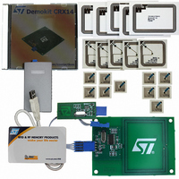
RFID EVALUATION KIT ISO14443-B
Manufacturer
STMicroelectronics
Type
Development kitr
Specifications of DEMOKITCRX14
Contents
CD-ROM, CRX14 Board, USB Transceiver, Samples and Documentation
Processor To Be Evaluated
CRX14
Interface Type
I2C
Operating Supply Voltage
5 V
For Use With/related Products
CRX14
Lead Free Status / RoHS Status
Contains lead / RoHS non-compliant
Other names
497-3704
Available stocks
Company
Part Number
Manufacturer
Quantity
Price
Company:

Part Number:
DEMOKITCRX14
Manufacturer:
HITACHI
Quantity:
340


CRX14
3.2
Table 3.
1. RFU = Reserved for Future Use.
Input/output frame register (01h)
The Input/Output Frame Register is a 36-Byte buffer that is accessed serially from Byte 0
through to Byte 35 (see
The Input/Output Frame Register is the buffer in which the CRX14 stores the data Bytes of
the request frame to be sent to the PICC. It automatically stores the data Bytes of the
answer frame received from the PICC. The first Byte (Byte 0) of the Input/Output Frame
Register is used to store the frame length for both transmission and reception.
When accessed in I²C Write mode , the register stores the request frame Bytes that are to
be transmitted to the PICC. Byte 0 must be set with the request frame length (in Bytes) and
the frame is stored from Byte 1 onwards. At the end of the transmission, the 16-bit CRC is
automatically added. After the transmission, the CRX14 wait for the PICC to send back an
answer frame. When correctly decoded, the PICC answer frame Bytes are stored in the
Input/Output Frame Register from Byte 1 onwards. Byte 0 stores the number of Bytes
received from the PICC.
When accessed in I²C Read mode, the Input/Output Register sends back the last PICC
answer frame Bytes, if any, with Byte 0 transmitted first. The 16-bit CRC is not stored, and it
is not sent back on the I²C bus.
The Input/Output Frame Register is set to all 00h between transmission and reception. If
there is no answer from the PICC, Byte 0 is set to 00h. In the case of a CRC error, Byte 0 is
set to FFh, and the data Bytes are discarded and not appended in the register.
The CRX14 Input/Output Frame Register is so designed as to generate all the ST short
range memory command frames. It can also generate all standardized ISO14443 type-B
command frames like REQB, SLOT-MARKER, ATTRIB, HALT, and get all the answers like
ATQB, or answer to ATTRIB. All ISO14443 type-B compliant PICCs can be accessed by the
CRX14 provided that their data frame exchange is not longer than 35 Bytes in both request
and answer.
b
b
b
b
b
b
Bit
2
3
4
5
6
7
Answer Frame Format
ASK Modulation Depth
Carrier Frequency
t
Answer delay watchdog
RFU
WDG
Parameter register bits description (continued)
Control
Table
0
Value
0
1
0
1
0
1
b5=0, b6=0: Watchdog time-out = 500µs to be used for read
b5=0, b6=1: Watchdog time-out = 5ms to be used for authentication
b5=1, b6=0: Watchdog time-out = 10ms to be used for write
b5=1, b6=1: Watchdog time-out = 309ms to be used for MCU timings
4). It is located at the I²C address 01h.
Doc ID 8880 Rev 4
Answer PICC Frames are delimited by SOF and EOF
Answer PICC Frames do not provide SOF and EOF
delimiters
10% ASK modulation depth mode
RFU
13.56MHz carrier on RF OUT is OFF
13.56MHz carrier on RF OUT is ON
Not used
Description
CRX14 registers
13/47
Related parts for DEMOKITCRX14
Image
Part Number
Description
Manufacturer
Datasheet
Request
R

Part Number:
Description:
DEMO KIT M24LR-64-R
Manufacturer:
STMicroelectronics
Datasheet:

Part Number:
Description:
STMicroelectronics [RIPPLE-CARRY BINARY COUNTER/DIVIDERS]
Manufacturer:
STMicroelectronics
Datasheet:
Part Number:
Description:
STMicroelectronics [LIQUID-CRYSTAL DISPLAY DRIVERS]
Manufacturer:
STMicroelectronics
Datasheet:

Part Number:
Description:
BOARD EVAL FOR MEMS SENSORS
Manufacturer:
STMicroelectronics
Datasheet:
Part Number:
Description:
NPN TRANSISTOR POWER MODULE
Manufacturer:
STMicroelectronics
Datasheet:
Part Number:
Description:
TURBOSWITCH ULTRA-FAST HIGH VOLTAGE DIODE
Manufacturer:
STMicroelectronics
Datasheet:
Part Number:
Description:
Manufacturer:
STMicroelectronics
Datasheet:
Part Number:
Description:
DIODE / SCR MODULE
Manufacturer:
STMicroelectronics
Datasheet:
Part Number:
Description:
DIODE / SCR MODULE
Manufacturer:
STMicroelectronics
Datasheet:
Part Number:
Description:
Search -----> STE16N100
Manufacturer:
STMicroelectronics
Datasheet:
Part Number:
Description:
Search ---> STE53NA50
Manufacturer:
STMicroelectronics
Datasheet:
Part Number:
Description:
NPN Transistor Power Module
Manufacturer:
STMicroelectronics
Datasheet: