DEMOKITCRX14 STMicroelectronics, DEMOKITCRX14 Datasheet - Page 10
DEMOKITCRX14
Manufacturer Part Number
DEMOKITCRX14
Description
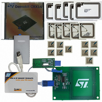
RFID EVALUATION KIT ISO14443-B
Manufacturer
STMicroelectronics
Type
Development kitr
Specifications of DEMOKITCRX14
Contents
CD-ROM, CRX14 Board, USB Transceiver, Samples and Documentation
Processor To Be Evaluated
CRX14
Interface Type
I2C
Operating Supply Voltage
5 V
For Use With/related Products
CRX14
Lead Free Status / RoHS Status
Contains lead / RoHS non-compliant
Other names
497-3704
Available stocks
Company
Part Number
Manufacturer
Quantity
Price
Company:

Part Number:
DEMOKITCRX14
Manufacturer:
HITACHI
Quantity:
340


Signal description
2.6
2.7
2.8
Figure 4.
10/47
V
CC
E0
OPT
R1
0R
R2
E1
OPT
R3
0R
R4
OPT
R5
0R
R6
Serial data (SDA)
The SDA signal is bi-directional. It is used to transfer I²C data in and out of the CRX14. It is
an open drain output that may be wire-OR’ed with other open drain or open collector signals
on the bus. A pull-up resistor must be connected from Serial data (SDA) to V
indicates how the value of the pull-up resistor can be calculated).
Chip enable (E0, E1, E2)
The Chip Enable inputs E0, E1, E2 are used to set and reset the value on the three least
significant bits (b3, b2, b1) of the 7-bit I²C Device Select Code. They are used for hardwired
addressing, allowing up to eight CRX14 devices to be addressed on the same I²C bus.
These inputs may be driven dynamically or tied to V
Select Code (note that the V
compatible).
When left open, E0, E1 and E2 are internally read at the logic level 0 due to the internal pull-
down resistors connected to each inputs.
Power supply (V
Power is supplied to the CRX14 using the V
V
The GND and GND_RF pins are ground connections. They must be connected together.
Decoupling capacitors should be connected between the V
Ground pin and the GND_REF Ground pin to filter the power line, as shown in
CRX14 application schematic
E2
CC
C3
22nF50V
is the Power Supply pin that supplies the power (+5V) for all CRX14 operations.
WURTH 742-792-042
FL7
1
2
3
4
5
6
7
8
4
3
2
1
U1
CRX14
J1
V
RF
E0
E1
E2
GND_RF
GND
GND
REF
IN
GND_RF
RF
FL5 0R
FL4
FL6
OSC1
OSC2
GND
V
SDA
OUT
SCL
CC
0R
0R
CC
C6
100nF50V
16
15
14
13
12
11
10
9
V
CC
SDA
, GND, GND_RF)
IL
SCL
and V
Doc ID 8880 Rev 4
V
CC
+ C4
22uF 10V
IH
C2 7pF50V
levels for the inputs are CMOS compatible, not TTL
C1 7pF50V
X1
13.56MHz
CC
, GND and GND_RF pins.
C8'
C8
8pF50V
100pF50V
CC
C7
120pF50V
or GND to establish the Device
CC
C7'
33pF50V
Supply Voltage pin, the GND
C5
10pF50V
D1
1N4148 (OPTIONAL)
R7
0R
R8
0R
ANT2
ANT1
CC
Figure
.
(Figure 5
CRX14
AI10952
4.
Related parts for DEMOKITCRX14
Image
Part Number
Description
Manufacturer
Datasheet
Request
R

Part Number:
Description:
DEMO KIT M24LR-64-R
Manufacturer:
STMicroelectronics
Datasheet:

Part Number:
Description:
STMicroelectronics [RIPPLE-CARRY BINARY COUNTER/DIVIDERS]
Manufacturer:
STMicroelectronics
Datasheet:
Part Number:
Description:
STMicroelectronics [LIQUID-CRYSTAL DISPLAY DRIVERS]
Manufacturer:
STMicroelectronics
Datasheet:

Part Number:
Description:
BOARD EVAL FOR MEMS SENSORS
Manufacturer:
STMicroelectronics
Datasheet:
Part Number:
Description:
NPN TRANSISTOR POWER MODULE
Manufacturer:
STMicroelectronics
Datasheet:
Part Number:
Description:
TURBOSWITCH ULTRA-FAST HIGH VOLTAGE DIODE
Manufacturer:
STMicroelectronics
Datasheet:
Part Number:
Description:
Manufacturer:
STMicroelectronics
Datasheet:
Part Number:
Description:
DIODE / SCR MODULE
Manufacturer:
STMicroelectronics
Datasheet:
Part Number:
Description:
DIODE / SCR MODULE
Manufacturer:
STMicroelectronics
Datasheet:
Part Number:
Description:
Search -----> STE16N100
Manufacturer:
STMicroelectronics
Datasheet:
Part Number:
Description:
Search ---> STE53NA50
Manufacturer:
STMicroelectronics
Datasheet:
Part Number:
Description:
NPN Transistor Power Module
Manufacturer:
STMicroelectronics
Datasheet: