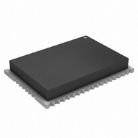
ATZB-24-A2 Atmel, ATZB-24-A2 Datasheet - Page 8

ATZB-24-A2
Manufacturer Part Number
ATZB-24-A2
Description
KIT MOD 802.15.4/ZIGB 2.4GHZ ANT
Manufacturer
Atmel
Specifications of ATZB-24-A2
Frequency
2.4GHz
Data Rate - Maximum
250kbps
Modulation Or Protocol
802.15.4 Zigbee
Applications
Home/Building Automation, Industrial Control and Monitoring
Power - Output
3dBm
Sensitivity
-101dBm
Voltage - Supply
1.8 V ~ 3.6 V
Current - Receiving
19mA
Current - Transmitting
18mA
Data Interface
PCB, Surface Mount
Memory Size
128kBytes Flash, 8kBytes RAM, 4kBytes EEPROM
Antenna Connector
On-Board, Chip
Operating Temperature
-40°C ~ 85°C
Package / Case
Module
Tool Type
Wireless Development Kit
Core Architecture
AVR
Cpu Core
AVR 8
Data Bus Width
8 bit
Description/function
ZigBit 2.4 GHz Dual Chip Antenna
Wireless Frequency
2.4 GHz
Interface Type
UART, I2C, SPI
Operating Voltage
1.8 V to 3.6 V
Output Power
3 dBm
Antenna
Chip Antenna
Operating Temperature Range
- 40 C to + 85 C
Lead Free Status / RoHS Status
Lead free / RoHS Compliant
Available stocks
Company
Part Number
Manufacturer
Quantity
Price
Part Number:
ATZB-24-A2
Manufacturer:
ATMEL/爱特梅尔
Quantity:
20 000
Company:
Part Number:
ATZB-24-A2R
Manufacturer:
CIRRUS
Quantity:
201
6. AVR CPU
6.1
6.2
8069Q–AVR–12/10
Features
Overview
•
•
•
•
•
•
•
•
The XMEGA A4 uses the 8/16-bit AVR CPU. The main function of the CPU is program execu-
tion. The CPU must therefore be able to access memories, perform calculations and control
peripherals. Interrupt handling is described in a separate section.
the CPU block diagram.
Figure 6-1.
The AVR uses a Harvard architecture - with separate memories and buses for program and
data. Instructions in the program memory are executed with a single level pipeline. While one
instruction is being executed, the next instruction is pre-fetched from the program memory. This
8/16-bit high performance AVR RISC Architecture
32x8-bit registers directly connected to the ALU
Stack in RAM
Stack Pointer accessible in I/O memory space
Direct addressing of up to 16M Bytes of program and data memory
True 16/24-bit access to 16/24-bit I/O registers
Support for 8-, 16- and 32-bit Arithmetic
Configuration Change Protection of system critical features
– 138 instructions
– Hardware multiplier
Peripheral
Module 1
CPU block diagram
CONTROL
STATUS/
Program
Counter
OCD
Peripheral
Module 2
Instruction
Instruction
Program
Register
Memory
Decode
Flash
DATA BUS
SRAM
DATA BUS
ALU
EEPROM
32 x 8 General
Registers
Multiplier/
Purpose
DES
Figure 6-1 on page 8
PMIC
XMEGA A4
shows
8


