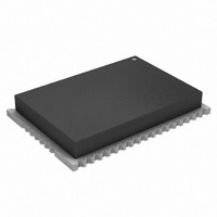
ATZB-24-A2 Atmel, ATZB-24-A2 Datasheet - Page 12

ATZB-24-A2
Manufacturer Part Number
ATZB-24-A2
Description
KIT MOD 802.15.4/ZIGB 2.4GHZ ANT
Manufacturer
Atmel
Specifications of ATZB-24-A2
Frequency
2.4GHz
Data Rate - Maximum
250kbps
Modulation Or Protocol
802.15.4 Zigbee
Applications
Home/Building Automation, Industrial Control and Monitoring
Power - Output
3dBm
Sensitivity
-101dBm
Voltage - Supply
1.8 V ~ 3.6 V
Current - Receiving
19mA
Current - Transmitting
18mA
Data Interface
PCB, Surface Mount
Memory Size
128kBytes Flash, 8kBytes RAM, 4kBytes EEPROM
Antenna Connector
On-Board, Chip
Operating Temperature
-40°C ~ 85°C
Package / Case
Module
Tool Type
Wireless Development Kit
Core Architecture
AVR
Cpu Core
AVR 8
Data Bus Width
8 bit
Description/function
ZigBit 2.4 GHz Dual Chip Antenna
Wireless Frequency
2.4 GHz
Interface Type
UART, I2C, SPI
Operating Voltage
1.8 V to 3.6 V
Output Power
3 dBm
Antenna
Chip Antenna
Operating Temperature Range
- 40 C to + 85 C
Lead Free Status / RoHS Status
Lead free / RoHS Compliant
Available stocks
Company
Part Number
Manufacturer
Quantity
Price
Part Number:
ATZB-24-A2
Manufacturer:
ATMEL/爱特梅尔
Quantity:
20 000
Company:
Part Number:
ATZB-24-A2R
Manufacturer:
CIRRUS
Quantity:
201
7.4
Figure 7-2.
7.4.1
7.4.2
8069Q–AVR–12/10
Byte Address
Data Memory
I/O Memory
SRAM Data Memory
2FFF
17FF
1000
2000
FFF
Data Memory Map (Hexadecimal address)
0
ATxmega64A4
Internal SRAM
I/O Registers
RESERVED
EEPROM
(4 KB)
(2 KB)
(4 KB)
The Data Memory consist of the I/O Memory, EEPROM and SRAM memories, all within one lin-
ear address space, see
devices in the family is identical and with empty, reserved memory space for smaller devices.
All peripherals and modules are addressable through I/O memory locations in the data memory
space. All I/O memory locations can be accessed by the Load (LD/LDS/LDD) and Store
(ST/STS/STD) instructions, transferring data between the 32 general purpose registers in the
CPU and the I/O Memory.
The IN and OUT instructions can address I/O memory locations in the range 0x00 - 0x3F
directly.
I/O registers within the address range 0x00 - 0x1F are directly bit-accessible using the SBI and
CBI instructions. The value of single bits can be checked by using the SBIS and SBIC instruc-
tions on these registers.
The I/O memory address for all peripherals and modules in XMEGA A4 is shown in the
eral Module Address Map” on page
The XMEGA A4 devices have internal SRAM memory for data storage.
Byte Address
Figure 7-2 on page
2FFF
13FF
1000
2000
FFF
0
53.
ATxmega32A4
Internal SRAM
I/O Registers
RESERVED
EEPROM
(4 KB)
(1 KB)
(4 KB)
12. To simplify development, the memory map for all
Byte Address
Byte Address
3FFF
17FF
1000
2000
13FF
27FF
FFF
1000
2000
FFF
0
0
XMEGA A4
ATxmega128A4
Internal SRAM
ATxmega16A4
Internal SRAM
I/O Registers
I/O Registers
RESERVED
EEPROM
RESERVED
EEPROM
(4 KB)
(2 KB)
(8 KB)
(4 KB)
(1 KB)
(2 KB)
”Periph-
12


