ETRX2 Telegesis Ltd, ETRX2 Datasheet - Page 16
ETRX2
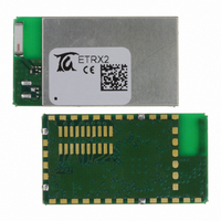
Manufacturer Part Number
ETRX2
Description
MODULE ZIGBEE EM250 CHIP ANT
Manufacturer
Telegesis Ltd
Specifications of ETRX2
Frequency
2.4GHz
Data Rate - Maximum
250kbps
Modulation Or Protocol
802.15.4 Zigbee
Applications
ISM
Power - Output
3dBm
Sensitivity
-98dBm
Voltage - Supply
2.1 V ~ 3.6 V
Current - Receiving
35.5mA
Current - Transmitting
35.5mA
Data Interface
PCB, Surface Mount
Memory Size
128kB Flash, 5kB SRAM
Antenna Connector
On-Board, Chip
Operating Temperature
-40°C ~ 85°C
Package / Case
Module
Module Applications
AMR, Building Automation, Wireless Sensor Network, M2M Industrial Controls
Mcu Supported Families
EM250
Processor Type
EM250
Wireless Protocol
IEEE 802.15.4
Data Rate
250Kbps
Module Interface
I2C, SPI, UART
Rohs Compliant
Yes
Lead Free Status / RoHS Status
Lead free / RoHS Compliant
Other names
920-1000-2


9 DC Electrical Characteristics
VBAT = 3.0V, T
1
2
3
4
5
6
7
8
9
10
11
12
13
14
15
16
17
18
19
20
21
22
23
Notes:
internal regulated core voltage at Vreg mainly feeds circuitry on ETRX2, the Vreg module pin may only be
slightly loaded and without feeding noise to Vreg. Vreg is not available in Power Mode 3 (see the AT
Command Manual for details of power modes).
Where the dc regulator option is mounted Vreg is connected to the regulator option output instead and the
internal regulated core voltage is not accessible.
©2009 Telegesis (UK) Ltd
No.
Module supply voltage VBAT
Internal regulated core
voltage
Quiescent current, including
internal RC oscillator
Quiescent current, including
32.768kHz oscillator
Transmit current consumption
Transmit current consumption
Transmit current consumption
Receive current consumption
Receive current consumption
External load on internal
regulated core voltage
Input voltage for logic 0
input voltage for logic 1
Input current for logic 0
input current for logic 1
input pull-up resistor value
input pull-down resistor value
Output voltage for logic 0
Output voltage for logic 1
Output source current
(standard current pad)
Output sink current
(standard current pad)
Output source current (high
current pad: I/O3, I/O1, I/O10,
I/O11 )
Output sink current (high
current pad: : I/O3, I/O1,
I/O10, I/O11)
Total output current
for I/O pads
For more information about the internal regulated core voltage refer to part 5.7 in [2]. As the
Item
amb
= 25°C unless otherwise stated
connected to
Vreg pad 5
10kΩ pull-down at
SIF_MOSI pin
10kΩ pull-down at
SIF_MOSI pin
total at +3dBm
maximum output
power
total at +5dBm
maximum output
power
at boost mode
total at -32dBm
minimum output
power
total
total (boost mode)
connected to
Vreg pad 5
Table 4: DC Electrical Characteristics
Condition /
Remark
(1)
(1)
- 16 -
V
V
I
I
I
I
I
I
I
I
V
V
I
I
R
R
V
V
I
I
I
I
I
I
Symbol
SLEEP
SLEEP
TX
TX
TX
RX
RX
REG_OUT
IL
IH
OHS
OLS
OHH
OLH
OH
OL
BAT
CORE
IL
IH
OL
OH
IPU
IPD
+
2.1
1.7
0
0.8x
VBAT
0
0.82x
VBAT
ETRX2 Product Manual (Rev 1.09)
Min
Value
3.0
1.8
35.5
41.5
28
35.5
37.5
30
30
Typ
3.6
1.9
1.0
1.5
2
0.2x
VBAT
VBAT
-0.5
0.5
0.18x
VBAT
VBAT
4
4
8
8
40
Max
Vdc
Vdc
µA
µA
mA
mA
mA
mA
mA
mA
Vdc
Vdc
µA
µA
kΩ
kΩ
Vdc
Vdc
mA
mA
mA
mA
mA
Unit
ETRX2
Related parts for ETRX2
Image
Part Number
Description
Manufacturer
Datasheet
Request
R

Part Number:
Description:
KIT DEVELOPMENT FOR ETRX357
Manufacturer:
Telegesis Ltd
Datasheet:

Part Number:
Description:
MODULE ZIGBEE USB STICK
Manufacturer:
Telegesis Ltd
Datasheet:

Part Number:
Description:
MODULE ZIGBEE PWR AMP USB STICK
Manufacturer:
Telegesis Ltd
Datasheet:

Part Number:
Description:
ZIGBEE ETHERNET ACCESS POINT
Manufacturer:
Telegesis Ltd
Datasheet:

Part Number:
Description:
ZIGBEE ETHERNET ACCESS POINT
Manufacturer:
Telegesis Ltd
Datasheet:

Part Number:
Description:
MODULE ZIGBEE EM357 W/CHIP ANT
Manufacturer:
Telegesis Ltd
Datasheet:

Part Number:
Description:
MODULE ZIGBEE W/PWR AMP
Manufacturer:
Telegesis Ltd
Datasheet:
Part Number:
Description:
MODULE ZIGBEE W/PA LNA CHIP ANT
Manufacturer:
Telegesis Ltd
Datasheet:
Part Number:
Description:
MODULE ZIGBEE W/PA LNA U.FL
Manufacturer:
Telegesis Ltd
Datasheet:
Part Number:
Description:
MODULE, ZIGBEE, ETRX351, CHIP ANT
Manufacturer:
Telegesis Ltd
Datasheet:
Part Number:
Description:
MODULE, ZIGBEE, ETRX3, HIROSE
Manufacturer:
Telegesis Ltd
Datasheet:
Part Number:
Description:
MODULE, ZIGBEE, ETRX3, PA+LNA, CHIP
Manufacturer:
Telegesis Ltd
Datasheet:
Part Number:
Description:
MODULE, ZIGBEE, ETRX3, PA+LNA, HIROS
Manufacturer:
Telegesis Ltd
Datasheet:
Part Number:
Description:
MODULE, ZIGBEE, ETRX351, HIROSE
Manufacturer:
Telegesis Ltd
Datasheet:
Part Number:
Description:
MODULE
Manufacturer:
Telegesis Ltd
Datasheet: