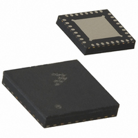
MC13202FCR2 Freescale Semiconductor, MC13202FCR2 Datasheet - Page 23

MC13202FCR2
Manufacturer Part Number
MC13202FCR2
Description
IC TXRX RF 2.4GHZ 32-QFN
Manufacturer
Freescale Semiconductor
Datasheet
1.MC13202FCR2.pdf
(30 pages)
Specifications of MC13202FCR2
Frequency
2.4GHz
Data Rate - Maximum
250kbps
Modulation Or Protocol
802.15.4
Applications
AMR, HID, HVAC, ISM
Power - Output
-27dBm ~ 3dBm
Sensitivity
-92dBm
Voltage - Supply
2 V ~ 3.4 V
Current - Receiving
37mA
Current - Transmitting
30mA
Data Interface
PCB, Surface Mount
Antenna Connector
PCB, Surface Mount
Operating Temperature
-40°C ~ 85°C
Package / Case
32-QFN
Operating Temperature (min)
-40C
Operating Temperature (max)
85C
Operating Temperature Classification
Industrial
Lead Free Status / RoHS Status
Lead free / RoHS Compliant
Memory Size
-
Lead Free Status / Rohs Status
Compliant
Other names
MC13202FCR2
MC13202FCR2TR
MC13202FCR2TR
9.1.1
The integrated RF switch allows users to operate in a single port configuration. For Single Port Mode:
Figure 13
The CT_Bias is connected to the balun center-tap providing the proper DC bias voltage to the balun
depending on RX or TX.
9.1.2
A second set of pins designated PAO_P and PAO_N allow operation in a dual port configuration. There
are separate paths for transmit and receive with the optional CT_Bias pin providing a signal that indicates
if the radio is in TX or RX Mode which then can be used to drive an external low noise amplifier, power
amplifier, or antenna switch.
In dual port operation, the RFIN_P and RFIN_N are inputs only, the internal RX switch to the LNA is
enabled to receive, and the associated TX PA stays disabled. Pins PAO_P and PAO_N become the
differential output pins and the associated TX PA is enabled for transmit.
Freescale Semiconductor
•
•
•
•
An internal RX switch and separate PA are used and pins RFIN_P (PAO_P) and RFIN_M
(PAO_M) become bidirectional and connect both for TX and RX
When receiving, the RX switch is enabled to the internal LNA and the TX PA is disabled.
When transmitting, the RX switch is disabled (isolating the LNA) and a TX PA is enabled.
The optional CT_Bias pin provides a control signal or bias voltage
— Switches between VDDA (nominal 1.8Vdc) and ground
— When used with a balun provides a high reference or bias voltage which is at VDDA for
— Can also be used a control signal for external components (note VDDA is only active high
shows a single port example with a balun.
transmit and is at ground for receive. This is the proper bias voltage to the balun that converts
a single-ended antenna to the differential interface required by the transceiver.
when a CCA, RX, or TX sequence is in progress)
Single Port Operation
Dual Port Operation
Figure 13. Single Port RF Operation with a Balun
Balun
MC13202 Technical Data, Rev. 1.5
Bypass
MC13202/03
L1
RFIN_M (PAO_M)
PAO_M
RFIN_P (PAO_P)
CT_Bias
PAO_P
23


