MC13202FCR2 Freescale Semiconductor, MC13202FCR2 Datasheet - Page 22
MC13202FCR2
Manufacturer Part Number
MC13202FCR2
Description
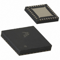
IC TXRX RF 2.4GHZ 32-QFN
Manufacturer
Freescale Semiconductor
Datasheet
1.MC13202FCR2.pdf
(30 pages)
Specifications of MC13202FCR2
Frequency
2.4GHz
Data Rate - Maximum
250kbps
Modulation Or Protocol
802.15.4
Applications
AMR, HID, HVAC, ISM
Power - Output
-27dBm ~ 3dBm
Sensitivity
-92dBm
Voltage - Supply
2 V ~ 3.4 V
Current - Receiving
37mA
Current - Transmitting
30mA
Data Interface
PCB, Surface Mount
Antenna Connector
PCB, Surface Mount
Operating Temperature
-40°C ~ 85°C
Package / Case
32-QFN
Operating Temperature (min)
-40C
Operating Temperature (max)
85C
Operating Temperature Classification
Industrial
Lead Free Status / RoHS Status
Lead free / RoHS Compliant
Memory Size
-
Lead Free Status / Rohs Status
Compliant
Other names
MC13202FCR2
MC13202FCR2TR
MC13202FCR2TR


9
The MC13202 radio has features that allow for a flexible as well as low cost RF interface:
9.1
Figure 12
associated with RFIN_x and PAO_x signal pairs. The RF interface allows both single port differential
operation and dual port differential operation.
22
•
•
•
•
•
•
— MC9S08GT devices have IO signals that are not pinned-out on the package. These signals must
Transceiver RF Configurations and External
Connections
Programmable output power — 0 dBm nominal output power, programmable from -27 dBm to +4
dBm typical
<-94 dBm (typical) receive sensitivity — At 1% PER, 20-byte packet (well above 802.15.4
Standard of -85 dBm)
Optional integrated transmit/receive (T/R) switch for low cost operation — With internal PAs and
LNA, the internal T/R switch allows a minimal part count radio interface using only a single balun
to interface to a single-ended antenna
Maximum flexibility — There are full differential RF I/O pins for use with the internal T/R switch.
Optionally, these pins become the RF_IN signals and a separate set of full differential PA outputs
are also provided. Separate inputs and outputs allow for a variety of RF configurations including
external LNA and PA for increased range
CT_Bias Output — The CT_Bias signal provides a switched bias reference for use with the internal
T/R switch, and alternatively can be programmed as an antenna switch signal for use with an
external antenna switch
Onboard trim capability for 16 MHz crystal reference oscillator — The 802.15.4 Standard puts a
+/- 40 ppm requirement on the carrier frequency. The onboard trim capability of the modem crystal
oscillator eliminates need for external variable capacitors and allows for automated production
frequency calibration. Also tighter tolerance can produce greater receive sensitivity
RF Interface Pins
shows the RF interface pins and the associated analog blocks. Notice that separate PA blocks are
also be initialized (even though they cannot be used) to prevent floating inputs.
2
1
3
5
6
R F IN _ M (P A O _ M )
C T _ B ia s
R F IN _ P (P A O _ P )
P A O _ M
P A O _ P
P A 1
MC13202 Technical Data, Rev. 1.5
Figure 12. RF Interface Pins
P A 2
F R O M T X P S M
C T _ B ia s C O N T R O L
P A 1 E N A B L E
P A 2 E N A B L E
C T _ B ia s G e n e r a to r
S W IT C H
R X
R X E N A B L E
L N A
S IG N A L
R X
Freescale Semiconductor
Related parts for MC13202FCR2
Image
Part Number
Description
Manufacturer
Datasheet
Request
R

Part Number:
Description:
Mc13203 2.4ghz Rf Transceiver For Zigbee Applications
Manufacturer:
Freescale Semiconductor, Inc
Datasheet:

Part Number:
Description:
Manufacturer:
Freescale Semiconductor, Inc
Datasheet:
Part Number:
Description:
Manufacturer:
Freescale Semiconductor, Inc
Datasheet:
Part Number:
Description:
Manufacturer:
Freescale Semiconductor, Inc
Datasheet:
Part Number:
Description:
Manufacturer:
Freescale Semiconductor, Inc
Datasheet:
Part Number:
Description:
Manufacturer:
Freescale Semiconductor, Inc
Datasheet:
Part Number:
Description:
Manufacturer:
Freescale Semiconductor, Inc
Datasheet:
Part Number:
Description:
Manufacturer:
Freescale Semiconductor, Inc
Datasheet:
Part Number:
Description:
Manufacturer:
Freescale Semiconductor, Inc
Datasheet:
Part Number:
Description:
Manufacturer:
Freescale Semiconductor, Inc
Datasheet:
Part Number:
Description:
Manufacturer:
Freescale Semiconductor, Inc
Datasheet:
Part Number:
Description:
Manufacturer:
Freescale Semiconductor, Inc
Datasheet:
Part Number:
Description:
Manufacturer:
Freescale Semiconductor, Inc
Datasheet: