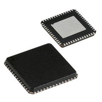
CYRF69103-40LFXC Cypress Semiconductor Corp, CYRF69103-40LFXC Datasheet - Page 6

CYRF69103-40LFXC
Manufacturer Part Number
CYRF69103-40LFXC
Description
IC PROC 8K FLASH 40VQFN
Manufacturer
Cypress Semiconductor Corp
Series
CYRFr
Datasheet
1.CYRF69103-40LFXC.pdf
(68 pages)
Specifications of CYRF69103-40LFXC
Package / Case
40-VQFN Exposed Pad, 40-HVQFN, 40-SQFN, 40-DHVQFN
Frequency
2.4GHz
Data Rate - Maximum
1Mbps
Modulation Or Protocol
ISM
Applications
General Purpose
Power - Output
6dBm
Sensitivity
-87dBm
Voltage - Supply
1.8 V ~ 3.6 V
Current - Receiving
21.9mA
Current - Transmitting
39.9mA
Data Interface
PCB, Surface Mount
Memory Size
8kB Flash, 256B SRAM
Antenna Connector
PCB, Surface Mount
Operating Temperature
0°C ~ 70°C
Processor Series
CYRF691x
Core
M8C
Data Bus Width
8 bit
Data Ram Size
256 B
Interface Type
SPI
Maximum Clock Frequency
2 MHz
Number Of Programmable I/os
15
Number Of Timers
4
Operating Supply Voltage
2.5 V, 3.3 V
Maximum Operating Temperature
+ 70 C
Mounting Style
SMD/SMT
Minimum Operating Temperature
0 C
Program Memory Type
Flash
Program Memory Size
8 KB
Operating Temperature (min)
0C
Operating Temperature (max)
70C
Operating Temperature Classification
Commercial
Operating Supply Voltage (min)
1.8V
Operating Supply Voltage (typ)
2.5/3.3V
Operating Supply Voltage (max)
3.6V
Height
1 mm
Length
5.9 mm
Supply Voltage (max)
3.6 V
Supply Voltage (min)
1.8 V
Width
5.9 mm
Lead Free Status / RoHS Status
Lead free / RoHS Compliant
For Use With
770-1001 - ISP 4PORT CYPRESS ENCORE II MCU
Lead Free Status / Rohs Status
Lead free / RoHS Compliant
Other names
428-1933
Available stocks
Company
Part Number
Manufacturer
Quantity
Price
Part Number:
CYRF69103-40LFXC
Manufacturer:
CYCRESS
Quantity:
20 000
7. Pinouts
Table 7-1. Pin Definitions
Document #: 001-07611 Rev *F
14, 17, 18, 20
3, 7, 16
Pin
10
12
13
15
19
21
22
23
24
25
26
27
28
29
30
11
1
2
4
5
6
8
9
P1.5 / MOSI
P1.4 / SCK
P1.3 / nSS
V
DD_micro
Name
RF
RESV
XOUT
MISO
XTAL
V
V
GND
P0.4
P0.3
P0.1
P2.1
P2.0
P1.0
P1.1
P1.2
V
RF
RF
IRQ
NC
bat1
bat2
CC
bias
p
n
Individually configured GPIO
12 MHz crystal
2.4V to 3.6V supply. Connected to pin 40 (0.047 μF bypass)
Individually configured GPIO
Individually configured GPIO
Connect to 1.8V to 3.6V power supply, through 47 ohm series/1 μF shunt C
GPIO. Port 2 Bit 1
Connected to1.8V to 3.6V main power supply, through 0.047 μF bypass C
RF pin voltage reference
Differential RF to or from antenna
GND
Differential RF to or from antenna
GPIO
Reserved. Must connect to GND
GPIO
GPIO
MCU supply connected to pin 40, max CPU 12 MHz
GPIO
Slave Select
SPI Clock
Radio Function Interrupt output, configure High, Low or as Radio GPIO
MOSI pin from microcontroller function to radio function
3-wire SPI mode configured as Radio GPIO. In 4-wire SPI mode sends data to MCU function
Buffered CLK, PACTL_n or Radio GPIO
RF
XTAL
V
V
P0.4
P0.3
P0.1
P2.1
V
BAT1
V
BAT2
BIAS
Corner
tabs
CC
CC
10
1
2
3
4
5
6
7
8
9
Figure 7-1. Pin Diagram
WirelessUSB LP
CYRF69103
* E-PAD Bottom Side
Description
30
29
28
27
26
25
24
23
22
21
XOUT / GPIO
MISO / GPIO
P1.5 / MOSI
IRQ / GPIO
P1.4 / SCK
P1.3 / SS
P1.2
V
P1.1
P1.0
DD_Micro
CYRF69103
Page 6 of 68
[+] Feedback


