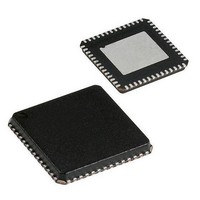
CYRF69103-40LFXC Cypress Semiconductor Corp, CYRF69103-40LFXC Datasheet - Page 52

CYRF69103-40LFXC
Manufacturer Part Number
CYRF69103-40LFXC
Description
IC PROC 8K FLASH 40VQFN
Manufacturer
Cypress Semiconductor Corp
Series
CYRFr
Datasheet
1.CYRF69103-40LFXC.pdf
(68 pages)
Specifications of CYRF69103-40LFXC
Package / Case
40-VQFN Exposed Pad, 40-HVQFN, 40-SQFN, 40-DHVQFN
Frequency
2.4GHz
Data Rate - Maximum
1Mbps
Modulation Or Protocol
ISM
Applications
General Purpose
Power - Output
6dBm
Sensitivity
-87dBm
Voltage - Supply
1.8 V ~ 3.6 V
Current - Receiving
21.9mA
Current - Transmitting
39.9mA
Data Interface
PCB, Surface Mount
Memory Size
8kB Flash, 256B SRAM
Antenna Connector
PCB, Surface Mount
Operating Temperature
0°C ~ 70°C
Processor Series
CYRF691x
Core
M8C
Data Bus Width
8 bit
Data Ram Size
256 B
Interface Type
SPI
Maximum Clock Frequency
2 MHz
Number Of Programmable I/os
15
Number Of Timers
4
Operating Supply Voltage
2.5 V, 3.3 V
Maximum Operating Temperature
+ 70 C
Mounting Style
SMD/SMT
Minimum Operating Temperature
0 C
Program Memory Type
Flash
Program Memory Size
8 KB
Operating Temperature (min)
0C
Operating Temperature (max)
70C
Operating Temperature Classification
Commercial
Operating Supply Voltage (min)
1.8V
Operating Supply Voltage (typ)
2.5/3.3V
Operating Supply Voltage (max)
3.6V
Height
1 mm
Length
5.9 mm
Supply Voltage (max)
3.6 V
Supply Voltage (min)
1.8 V
Width
5.9 mm
Lead Free Status / RoHS Status
Lead free / RoHS Compliant
For Use With
770-1001 - ISP 4PORT CYPRESS ENCORE II MCU
Lead Free Status / Rohs Status
Lead free / RoHS Compliant
Other names
428-1933
Available stocks
Company
Part Number
Manufacturer
Quantity
Price
Part Number:
CYRF69103-40LFXC
Manufacturer:
CYCRESS
Quantity:
20 000
Table 21-2. Interrupt Clear 0 (INT_CLR0) [0xDA] [R/W]
Table 21-3. Interrupt Clear 1 (INT_CLR1) [0xDB] [R/W]
Table 21-4. Interrupt Clear 2 (INT_CLR2) [0xDC] [R/W]
21.3.2 Interrupt Mask Registers
The Interrupt Mask Registers (INT_MSKx) are used to enable the individual interrupt sources’ ability to create pending interrupts.
There are four Interrupt Mask Registers (INT_MSK0, INT_MSK1, INT_MSK2, and INT_MSK3) that may be referred to in general as
INT_MSKx. If cleared, each bit in an INT_MSKx register prevents a posted interrupt from becoming a pending interrupt (input to the
priority encoder). However, an interrupt can still post even if its mask bit is zero. All INT_MSKx bits are independent of all other
INT_MSKx bits.
If an INT_MSKx bit is set, the interrupt source associated with that mask bit may generate an interrupt that becomes a pending
interrupt.
The Enable Software Interrupt (ENSWINT) bit in INT_MSK3[7] determines the way an individual bit value written to an INT_CLRx
register is interpreted. When is cleared, writing 1's to an INT_CLRx register has no effect. However, writing 0's to an INT_CLRx register,
when ENSWINT is cleared causes the corresponding interrupt to clear. If the ENSWINT bit is set, any 0's written to the INT_CLRx
registers are ignored. However, 1's written to an INT_CLRx register, while ENSWINT is set, cause an interrupt to post for the
corresponding interrupt.
Software interrupts can aid in debugging interrupt service routines by eliminating the need to create system level interactions that are
sometimes necessary to create a hardware-only interrupt.
Document #: 001-07611 Rev *F
When reading this register:
0 = There is no posted interrupt for the corresponding hardware.
1 = Posted interrupt for the corresponding hardware present.
Writing a ‘0’ to the bits clears the posted interrupts for the corresponding hardware. Writing a ‘1’ to the bits and to the ENSWINT
(Bit 7 of the INT_MSK3 Register) posts the corresponding hardware interrupt.
The GPIO interrupts are edge-triggered.
When reading this register:
0 = There is no posted interrupt for the corresponding hardware.
1 = Posted interrupt for the corresponding hardware present.
Writing a ‘0’ to the bits clears the posted interrupts for the corresponding hardware. Writing a ‘1’ to the bits AND to the ENSWINT.
Bit 7
When reading this register:
0 = There is no posted interrupt for the corresponding hardware
1 = Posted interrupt for the corresponding hardware present.
Writing a ‘0’ to the bits clears the posted interrupts for the corresponding hardware. Writing a ‘1’ to the bits AND to the ENSWINT
(Bit 7 of the INT_MSK3 Register) posts the corresponding hardware interrupt.
Bits 7,6,5,3,0]Reserved
Bit #
Field
Read/Write
Default
Bit #
Field
Read/Write
Default
Bit #
Field
Read/Write
Default
Reserved
GPIO Port 1 Sleep Timer
Reserved
Reserved
R/W
7
0
7
0
7
–
0
-
Prog Interval
Reserved
Timer
R/W
R/W
6
0
6
0
6
0
-
Reserved
Program-
Interrupt
mable
INT1
1 ms
R/W
R/W
5
0
5
0
5
0
-
GPIO Port 0 SPI Receive SPI Transmit
GPIO Port2
R/W
R/W
4
0
4
–
0
4
0
Reserved
R/W
3
0
3
–
0
3
–
0
Reserved
INT2
R/W
R/W
2
0
2
–
0
2
0
Reserved
Counter
16-bit
Wrap
R/W
R/W
1
0
1
–
0
1
0
CYRF69103
POR/LVD
Reserved
Page 52 of 68
R/W
0
0
0
–
0
0
0
-
[+] Feedback


