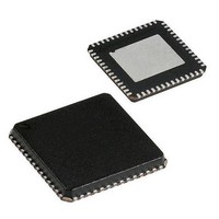
CYRF69103-40LFXC Cypress Semiconductor Corp, CYRF69103-40LFXC Datasheet - Page 11

CYRF69103-40LFXC
Manufacturer Part Number
CYRF69103-40LFXC
Description
IC PROC 8K FLASH 40VQFN
Manufacturer
Cypress Semiconductor Corp
Series
CYRFr
Datasheet
1.CYRF69103-40LFXC.pdf
(68 pages)
Specifications of CYRF69103-40LFXC
Package / Case
40-VQFN Exposed Pad, 40-HVQFN, 40-SQFN, 40-DHVQFN
Frequency
2.4GHz
Data Rate - Maximum
1Mbps
Modulation Or Protocol
ISM
Applications
General Purpose
Power - Output
6dBm
Sensitivity
-87dBm
Voltage - Supply
1.8 V ~ 3.6 V
Current - Receiving
21.9mA
Current - Transmitting
39.9mA
Data Interface
PCB, Surface Mount
Memory Size
8kB Flash, 256B SRAM
Antenna Connector
PCB, Surface Mount
Operating Temperature
0°C ~ 70°C
Processor Series
CYRF691x
Core
M8C
Data Bus Width
8 bit
Data Ram Size
256 B
Interface Type
SPI
Maximum Clock Frequency
2 MHz
Number Of Programmable I/os
15
Number Of Timers
4
Operating Supply Voltage
2.5 V, 3.3 V
Maximum Operating Temperature
+ 70 C
Mounting Style
SMD/SMT
Minimum Operating Temperature
0 C
Program Memory Type
Flash
Program Memory Size
8 KB
Operating Temperature (min)
0C
Operating Temperature (max)
70C
Operating Temperature Classification
Commercial
Operating Supply Voltage (min)
1.8V
Operating Supply Voltage (typ)
2.5/3.3V
Operating Supply Voltage (max)
3.6V
Height
1 mm
Length
5.9 mm
Supply Voltage (max)
3.6 V
Supply Voltage (min)
1.8 V
Width
5.9 mm
Lead Free Status / RoHS Status
Lead free / RoHS Compliant
For Use With
770-1001 - ISP 4PORT CYPRESS ENCORE II MCU
Lead Free Status / Rohs Status
Lead free / RoHS Compliant
Other names
428-1933
Available stocks
Company
Part Number
Manufacturer
Quantity
Price
Part Number:
CYRF69103-40LFXC
Manufacturer:
CYCRESS
Quantity:
20 000
8.12 Low Noise Amplifier (LNA) and Received
The gain of the receiver may be controlled directly by clearing
the AGC EN bit and writing to the Low Noise Amplifier (LNA) bit
of the RX_CFG_ADR register. When the LNA bit is cleared, the
receiver gain is reduced by approximately 20 dB, allowing
accurate reception of very strong received signals (for example
when operating a receiver very close to the transmitter). An
additional 20 dB of receiver attenuation can be added by setting
the Attenuation (ATT) bit; this allows data reception to be limited
to devices at very short ranges. Disabling AGC and enabling
LNA is recommended unless receiving from a device using
external PA.
The RSSI register returns the relative signal strength of the
on-channel signal power.
When receiving, the device may be configured to automatically
measure and store the relative strength of the signal being
received as a 5-bit value. When enabled, an RSSI reading is
taken and may be read through the SPI interface. An RSSI
reading is taken automatically when the start of a packet is
detected. In addition, a new RSSI reading is taken every time the
previous reading is read from the RSSI register, allowing the
background RF energy level on any given channel to be easily
measured when RSSI is read when no signal is being received.
A new reading can occur as fast as once every 12 μs.
9. SPI Interface
The SPI interface between the MCU function and the radio
function is a 3-wire SPI Interface. The three pins are MOSI
(Master Out Slave In), SCK (Serial Clock), SS (Slave Select).
There is an alternate 4-wire MISO Interface that requires the
connection of two external pins. The SPI interface is controlled
by configuring the SPI Configure Register. (SPICR Addr: 0x3D).
9.1 3-Wire SPI Interface
The radio function receives a clock from the MCU function on the
SCK pin. The MOSI pin is multiplexed with the MISO pin. Bidirec-
tional data transfer takes place between the MCU function and
the radio function through this multiplexed MOSI pin. When using
this mode the user firmware must ensure that the MOSI pin on
the MCU function is in a high impedance state, except when the
MCU is actively transmitting data. Firmware must also control the
direction of data flow and switch directions between MCU
function and radio function by setting the SWAP bit [Bit 7] of the
SPI Configure Register. The SS pin is asserted before initiating
a data transfer between the MCU function and the radio function.
The IRQ function may be optionally multiplexed with the MOSI
pin; when this option is enabled the IRQ function is not available
while the SS pin is low. When using this configuration, user
firmware must ensure that the MOSI function on MCU function
is in a high-impedance state whenever SS is high.
Document #: 001-07611 Rev *F
Signal Strength Indication (RSSI)
Figure 9-1. 3-Wire SPI Mode
9.2 4-Wire SPI Interface
The 4-wire SPI communications interface consists of MOSI,
MISO, SCK, and SS.
The device receives SCK from the MCU function on the SCK pin.
Data from the MCU function is shifted in on the MOSI pin. Data
to the MCU function is shifted out on the MISO pin. The active
low SS pin must be asserted for the two functions to commu-
nicate. The IRQ function may be optionally multiplexed with the
MOSI pin; when this option is enabled the IRQ function is not
available while the SS pin is low. When using this configuration,
user firmware must ensure that the MOSI function on MCU
function is in a high-impedance state whenever SS is high.
Figure 9-2. 4-Wire SPI Mode
MCU Function
P1.6/MISO
MCU Function
P1.5/MOSI
P1.4/SCK
P1.3/nSS
P1.5/MOSI
This connection is external to the PRoC LP Chip
P1.4/SCK
P1.3/nSS
MOSI/MISO multiplexed
on one MOSI pin
MOSI
nSS
SCK
SCK
MOSI
nSS
Radio Function
Radio Function
CYRF69103
Page 11 of 68
MISO
[+] Feedback


