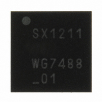
SX1211I084TRT Semtech, SX1211I084TRT Datasheet - Page 36

SX1211I084TRT
Manufacturer Part Number
SX1211I084TRT
Description
IC SNGL-CHIP TXRX 32-TQFN
Manufacturer
Semtech
Specifications of SX1211I084TRT
Frequency
860 ~ 960MHz
Data Rate - Maximum
200kbps
Modulation Or Protocol
FSK, OOK
Applications
AMR, ISM, Security and Access
Power - Output
12.5dBm
Sensitivity
-113dBm
Voltage - Supply
2.1 V ~ 3.6 V
Current - Receiving
3mA
Current - Transmitting
25mA
Data Interface
PCB, Surface Mount
Antenna Connector
PCB, Surface Mount
Operating Temperature
-40°C ~ 85°C
Package / Case
32-TQFN
Operating Temperature (min)
-40C
Operating Temperature (max)
85C
Operating Temperature Classification
Industrial
Modulation Type
FSK/OOK
Package Type
TQFN EP
Operating Supply Voltage (min)
2.1V
Operating Supply Voltage (typ)
2.5/3.3V
Operating Supply Voltage (max)
3.6V
Lead Free Status / RoHS Status
Lead free / RoHS Compliant
Memory Size
-
Lead Free Status / Rohs Status
Compliant
Other names
SX1211I084TRT
Available stocks
Company
Part Number
Manufacturer
Quantity
Price
Company:
Part Number:
SX1211I084TRT
Manufacturer:
HITTITE
Quantity:
560
Table 15: Config vs. Data SPI Interface Selection
The following paragraphs describe how to use each of these interfaces.
To write a value into a configuration register the timing diagram below should be carefully followed by the uC.
The register’s new value is effective from the rising edge of NSS_CONFIG.
Note that when writing more than one register successively, it is not compulsory to toggle NSS_CONFIG back high
between two write sequences. The bytes are alternatively considered as address and value. In this instance, all
new values will become effective on rising edge of NSS_CONFIG.
To read the value of a configuration register the timing diagram below should be carefully followed by the uC.
Rev 7 – Sept 2
ADVANCED COMMUNICATIONS & SENSING
NSS_CONFIG (In)
SCK (In)
MOSI (In)
MISO (Out)
Write Register
Read Register
NSS_DATA
0
0
1
1
nd
(input)
, 2008
HZ
* when writing the new value at address A1, the current content of A1 can be read by the uC.
5.2.1.2. SPI Config
NSS_CONFIG
0
1
0
1
start
1
x
rw
2
x
A(4) A(3) A(2) A(1)
3
x
SPI Interface
Config
Data
Config
None
Address = A1
4
x
Figure 27: Write Register Sequence
(In)/(Out) refers to SX1211 side
5
x
6
x
A(0)
Page 36 of 92
7
x
stop
8
x
D(7) D(6) D(5) D(4) D(3) D(2) D(1)
D(7) D(6) D(5) D(4) D(3) D(2) D(1) D(0)
9
10
11
Current value at
New value at
address A1
address A1*
12
13
14
15
www.semtech.com
16
D(0)
SX1211
(input)
HZ


