RXM-GPS-SR-T Linx Technologies Inc, RXM-GPS-SR-T Datasheet - Page 12
RXM-GPS-SR-T
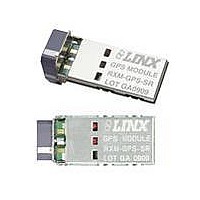
Manufacturer Part Number
RXM-GPS-SR-T
Description
GPS MODULE SMD SIRF W/ANT
Manufacturer
Linx Technologies Inc
Series
SRr
Type
GPS Receiver Moduler
Datasheet
1.MDEV-GPS-SR.pdf
(15 pages)
Specifications of RXM-GPS-SR-T
Package / Case
Module
Operating Voltage
3 V to 4.3 V
Operating Current
31 mA
Frequency Range
1575.42 MHz
Interface Type
UART, USB
Operating Temperature Range
- 30 C to + 85 C
Lead Free Status / RoHS Status
Lead free / RoHS Compliant
Features
-
Voltage - Supply
-
Frequency
-
Operating Temperature
-
Applications
-
Sensitivity
-
Memory Size
-
Data Interface
-
Data Rate - Maximum
-
Modulation Or Protocol
-
Antenna Connector
-
Current - Receiving
-
Lead Free Status / Rohs Status
Lead free / RoHS Compliant


BOARD LAYOUT GUIDELINES
Page 22
Page 22
The module’s design makes integration straightforward; however, it is still critical
to exercise care in PCB layout. Failure to observe good layout techniques can
result in degradation of the module’s performance. Grounding, filtering,
decoupling, routing and layer order are important considerations for any RF
design. The following section provides some basic design guidelines which may
be helpful.
During prototyping, the module should be soldered to a properly laid-out circuit
board. The use of prototyping or “perf” boards will result in poor performance and
is strongly discouraged.
The module should, as much as reasonably possible, be isolated from other
components on your PCB, especially high-frequency circuitry such as crystal
oscillators, switching power supplies, and high-speed bus lines.
When possible, separate RF and digital circuits into different PCB regions. Make
sure internal wiring is routed away from the module and antenna, and is secured
to prevent displacement.
Do not route PCB traces directly under the module. There should not be any
copper or traces under the module on the same layer as the module, just bare
PCB. The underside of the module has traces and vias that could short or couple
to traces on the product’s circuit board.
The Pad Layout section shows a typical PCB footprint for the module. A ground
plane (as large and uninterrupted as possible) should be placed on a lower layer
of your PC board opposite the module.
Vias are acceptable for tying together ground layers and should be used in
multiples.
Each of the module’s ground pins should have short traces tying immediately to
the ground plane through a via.
Bypass caps should be low ESR ceramic types and located directly adjacent to
the pin they are serving.
The integral antenna is susceptible to external influences. Please carefully read
and follow the guidelines listed in the section titled Antenna Considerations.
In some instances, a designer may wish to encapsulate or “pot” the product.
There is a wide variety of potting compounds with varying dielectric properties.
Since such compounds can considerably impact RF performance and the ability
to rework or service the product, it is the responsibility of the designer to evaluate
and qualify the impact and suitability of such materials. UNDER NO CONDITION
SHOULD THE ANTENNA ELEMENT BE POTTED OR ENCAPSULATED IN
ANY MANNER.
ANTENNA CONSIDERATIONS
Figure 6: Antenna Considerations
The SR Series module has an integral ceramic patch antenna. This eliminates
the need for any external RF components and, in some respects, simplifies the
design process. While convenient, an on-board antenna makes factors such as
layout, placement and product packaging much more critical. The antenna’s
performance plays a major role in determining realized sensitivity. In order for the
module to perform correctly it is essential that the antenna be given proper
consideration. Due to the compact size of the antenna, it may be necessary for
the antenna to be tuned specifically in the end product environment. If this is the
case, Linx can assist with layout and obtaining a custom tuned antenna.
Following these guidelines will help to achieve the best antenna performance.
The antenna element should be inside the product or covered to prevent damage
to it. The center frequency of the antenna will be affected by materials in close
proximity to it. The product’s housing should not come within approximately 0.25”
of any antenna surface. The housing must also be RF transparent, i.e. non-
metallic, no metal paint, fillers or compositions which would impede RF at the
frequencies of interest. The antenna should never be encapsulated, coated, or
sprayed with any compound.
Ideally, the antenna will sit at the edge of the PCB and have no other
components to the top or sides as illustrated below. If it is necessary to place
components adjacent to the antenna, try to maintain a 0.25” or greater setback
and recognize performance may be adversely affected. It is a good idea to test
your design’s performance against a benchmark. This will help to identify any
performance issues and the impact of design tradeoffs. A GPS module placed
on an optimized PCB with no external housing, or the Linx MDEV GPS
evaluation system, can be used as a helpful point of reference.
0.25” minimum clearance
on the top and sides
Locate the module
away from noise
generating or bearing
components or traces
Tie ground pins
individually to the
ground plane
Product PCB
Avoid placing components
to the sides of the module
No traces or copper
under the module on the
same layer as the module
Page 23
Page 23
Related parts for RXM-GPS-SR-T
Image
Part Number
Description
Manufacturer
Datasheet
Request
R

Part Number:
Description:
GPS MODULE SMD SIRF
Manufacturer:
Linx Technologies Inc
Datasheet:

Part Number:
Description:
GPS MODULE SMD SIRF W/ANT
Manufacturer:
Linx Technologies Inc
Datasheet:

Part Number:
Description:
GPS MODULE SMD SIRF
Manufacturer:
Linx Technologies Inc
Datasheet:

Part Number:
Description:
HOLDER BATTERY 20MM COIN CR2032
Manufacturer:
Linx Technologies Inc
Datasheet:

Part Number:
Description:
CONN RPSMA BL CRJA-CPV 8.5" COAX
Manufacturer:
Linx Technologies Inc

Part Number:
Description:
CABLE RG174 RPSMA M/F 8.5"
Manufacturer:
Linx Technologies Inc

Part Number:
Description:
CABLE RG174 SMA M/F 8.5"
Manufacturer:
Linx Technologies Inc

Part Number:
Description:
CABLE RPSMA/SMA 8.5"
Manufacturer:
Linx Technologies Inc

Part Number:
Description:
CABLE MALE-NMALE 8' RG-58 RPSMA
Manufacturer:
Linx Technologies Inc

Part Number:
Description:
CABLE RPSMA/SMA 8.5"
Manufacturer:
Linx Technologies Inc

Part Number:
Description:
MODULE USB LOW SPEED
Manufacturer:
Linx Technologies Inc
Datasheet:

Part Number:
Description:
IC TRANSCODER MT BI-DIR 20-SSOP
Manufacturer:
Linx Technologies Inc
Datasheet:

Part Number:
Description:
IC ENCODER LOW SECURITY 8DIP
Manufacturer:
Linx Technologies Inc
Datasheet:

Part Number:
Description:
IC DECODER MS SERIES 20-SSOP
Manufacturer:
Linx Technologies Inc
Datasheet:
Part Number:
Description:
IC ENCODER MS SERIES 20-SSOP
Manufacturer:
Linx Technologies Inc
Datasheet: