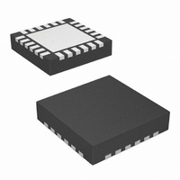
SI4313-B1-FM Silicon Laboratories Inc, SI4313-B1-FM Datasheet - Page 43

SI4313-B1-FM
Manufacturer Part Number
SI4313-B1-FM
Description
IC RX FSK 315-915MHZ 20VQFN
Manufacturer
Silicon Laboratories Inc
Series
EZRadio®r
Type
ISM Receiverr
Specifications of SI4313-B1-FM
Package / Case
20-VQFN
Mfg Application Notes
Si4313 Register Desc AppNote
Frequency
315MHz, 434MHz, 868MHz, 915MHz
Sensitivity
-118dBm
Data Rate - Maximum
128kbps
Modulation Or Protocol
FSK, GFSK, OOK
Applications
Data Logging, Health Monitors, Remote Control, Weather Station
Data Interface
PCB, Surface Mount
Antenna Connector
PCB, Surface Mount
Voltage - Supply
1.8 V ~ 3.6 V
Operating Temperature
-40°C ~ 85°C
Operating Frequency
315 MHz to 915 MHz
Operating Supply Voltage
1.8 V to 3.6 V
Maximum Operating Temperature
+ 85 C
Minimum Operating Temperature
- 40 C
Mounting Style
SMD/SMT
Supply Current
100 nA
Lead Free Status / RoHS Status
Lead free / RoHS Compliant
Features
-
Memory Size
-
Current - Receiving
-
Lead Free Status / Rohs Status
Lead free / RoHS Compliant
Other names
336-1980-5
Available stocks
Company
Part Number
Manufacturer
Quantity
Price
Company:
Part Number:
SI4313-B1-FMR
Manufacturer:
TI
Quantity:
10 000
Part Number:
SI4313-B1-FMR
Manufacturer:
SILICON LABS/芯科
Quantity:
20 000
12. Pin Descriptions: Si4313
PKG
Pin
2, 3
10
12
13
14
15
16
17
18
19
20
11
1
4
5
6
7
8
9
PADDLE_GND
Pin Name
VDD_DIG
VDD_RF
GPIO_0
GPIO_1
GPIO_2
XOUT
SCLK
nSEL
nIRQ
SDO
VDR
SDN
SDI
XIN
NC
RX
NC
NC
NC
GND
VDD
VDD
I/O
I/O
I/O
I/O
—
—
—
—
O
O
O
O
O
I
I
I
I
I
+1.8 to +3.6 V supply voltage input to all analog +1.7 V regulators. The recommended V
is +3.3 V.
No Connect.
RV input pin to LNA. See application schematic.
No Connect. Not connected internally to any circuitry.
No Connect
General Purpose Digital I/O that may be configured through the registers to perform various functions
including: Microcontroller Clock Output, FIFO status, POR, Wake-Up timer, Low Battery Detect, etc. See
the SPI GPIO Configuration Registers, Address 0Bh, 0Ch, and 0Dh for more information.
Regulated Output Voltage of the Digital 1.7 V Regulator. A 1 µF decoupling capacitor is required.
Internally this pin is tied to the paddle of the package. This pin should be left unconnected or connected to
GND only.
+1.8 to +3.6 V supply voltage input to the Digital +1.7 V Regulator. The recommended V
is +3.3 V.
0–V
Serial Data input. 0–V
bus.
Serial Clock input. 0–V
serial data bus. Data is clocked into the Si4313 on positive edge transitions.
Serial Interface Select input. 0– V
line serial data bus. The signal is also used to signify burst read/write mode.
General Microcontroller Interrupt Status output. When the Si4313 exhibits anyone of the Interrupt Events
the nIRQ pin will be set low=0. Please see the Control Logic registers section for more information on the
Interrupt Events. The Microcontroller can then determine the state of the interrupt by reading a corre-
sponding SPI Interrupt Status Registers, Address 03h and 04h. No external resistor pull-up is required,
but it may be desirable if multiple interrupt lines are connected.
Crystal Oscillator Output. Connect to an external 30 MHz crystal or to an external signal source.
Crystal Oscillator Input. Connect to an external 30 MHz crystal or leave floating if driving XOUT with
external signal source or TCXO.
Shutdown input pin. 0–V
SDN =1 the chip will be completely shutdown and the contents of the registers will be lost.
The exposed metal paddle on the bottom of the Si4313 supplies the RF and circuit ground(s) for the entire
chip. It is very important that a good solder connection is made between this exposed metal paddle and
the ground plane of the PCB underlying the Si4313.
DD
V digital output that provides a serial readback function of the internal control registers.
VDD
NC
NC
NC
RX
DD
2
3
4
5
1
6
DD
DD
V digital input. This pin provides the serial data stream for the 4-line serial data
V digital input. This pin provides the serial data clock function for the 4-line
20
7
V digital input. SDN should be = 0 in all modes except Shutdown mode. When
Rev. 1.0
19
GND
8
PAD
DD
18
9
V digital input. This pin provides the Select/Enable function for the 4-
17
10
16
11
15 SCLK
14
13
12
Description
SDI
SDO
VDD_DIG
NC
Si4313-B1
DD
DD
supply voltage
supply voltage
43


